MXenes for n- and p-type Ohmic contacts with Monolayer MoS2 and WS2: A first-principles study
IF 2.9
3区 物理与天体物理
Q3 NANOSCIENCE & NANOTECHNOLOGY
Physica E-low-dimensional Systems & Nanostructures
Pub Date : 2025-09-02
DOI:10.1016/j.physe.2025.116360
引用次数: 0
Abstract
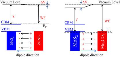
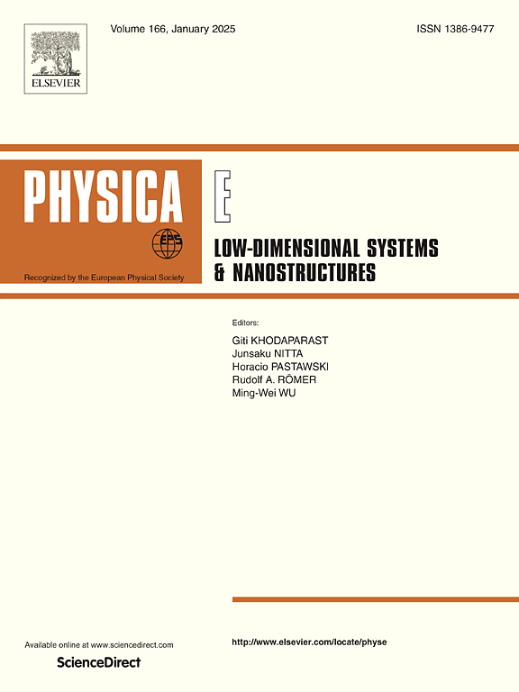
In the field of semiconductor devices, the contact characteristics between metal and semiconductor play a crucial role in determining device performance. Though first-principles calculations, systematic investigations on two prominent monolayer (ML) transition metal dichalcogenide (TMD) semiconductors, namely MoS2 and WS2, coupled with four ML MXene metals, are conducted. The TMD/MXene vertical heterojunctions exhibit van der Waals (vdW) type interactions, ensuring that the band structures of each component are well preserved. The formation of heterojunctions induces charge redistribution, which shifts the Fermi level. In the studied TMD/MXene vertical heterojunctions, the Fermi level shifts to the conduction or valence band edges of the ML semiconductor. Consequently, ML Zr2NF2 and Zr2N(OH)2 are identified as suitable n-type Ohmic contact electrodes for ML MoS2 and WS2, while ML Mo2CO2 serves as an effective p-type Ohmic contact electrode.
单层MoS2和WS2的n型和p型欧姆接触的MXenes:第一性原理研究
在半导体器件领域,金属与半导体的接触特性对器件的性能起着至关重要的作用。通过第一性原理计算,系统地研究了两种突出的单层(ML)过渡金属二硫化物(TMD)半导体,即MoS2和WS2,以及四种ML MXene金属。TMD/MXene垂直异质结表现出范德瓦尔斯(vdW)型相互作用,确保了每个组分的能带结构都得到了很好的保存。异质结的形成引起电荷再分布,从而使费米能级发生位移。在研究的TMD/MXene垂直异质结中,费米能级转移到ML半导体的导带或价带边缘。因此,ML Zr2NF2和Zr2N(OH)2是适合ML MoS2和WS2的n型欧姆接触电极,ML Mo2CO2是有效的p型欧姆接触电极。
本文章由计算机程序翻译,如有差异,请以英文原文为准。
求助全文
约1分钟内获得全文
求助全文
来源期刊
CiteScore
7.30
自引率
6.10%
发文量
356
审稿时长
65 days
期刊介绍:
Physica E: Low-dimensional systems and nanostructures contains papers and invited review articles on the fundamental and applied aspects of physics in low-dimensional electron systems, in semiconductor heterostructures, oxide interfaces, quantum wells and superlattices, quantum wires and dots, novel quantum states of matter such as topological insulators, and Weyl semimetals.
Both theoretical and experimental contributions are invited. Topics suitable for publication in this journal include spin related phenomena, optical and transport properties, many-body effects, integer and fractional quantum Hall effects, quantum spin Hall effect, single electron effects and devices, Majorana fermions, and other novel phenomena.
Keywords:
• topological insulators/superconductors, majorana fermions, Wyel semimetals;
• quantum and neuromorphic computing/quantum information physics and devices based on low dimensional systems;
• layered superconductivity, low dimensional systems with superconducting proximity effect;
• 2D materials such as transition metal dichalcogenides;
• oxide heterostructures including ZnO, SrTiO3 etc;
• carbon nanostructures (graphene, carbon nanotubes, diamond NV center, etc.)
• quantum wells and superlattices;
• quantum Hall effect, quantum spin Hall effect, quantum anomalous Hall effect;
• optical- and phonons-related phenomena;
• magnetic-semiconductor structures;
• charge/spin-, magnon-, skyrmion-, Cooper pair- and majorana fermion- transport and tunneling;
• ultra-fast nonlinear optical phenomena;
• novel devices and applications (such as high performance sensor, solar cell, etc);
• novel growth and fabrication techniques for nanostructures
 求助内容:
求助内容: 应助结果提醒方式:


