Fatima Matar, Xuefen Cai, Amar K. Salih, Ying-Li Shi, Kaludewa Sujeewa Buddhimali De Silva, Francis Chi Chung Ling, Matthew R. Phillips, Su-Huai Wei and Cuong Ton-That*,
{"title":"Band Gap Engineering and Electronic Property Modulation of β-Ga2O3 through Bi2O3 Alloying","authors":"Fatima Matar, Xuefen Cai, Amar K. Salih, Ying-Li Shi, Kaludewa Sujeewa Buddhimali De Silva, Francis Chi Chung Ling, Matthew R. Phillips, Su-Huai Wei and Cuong Ton-That*, ","doi":"10.1021/acs.jpcc.5c02687","DOIUrl":null,"url":null,"abstract":"<p >Bismuth (Bi) has recently emerged as a promising dopant for engineering the valence band of Ga<sub>2</sub>O<sub>3</sub> to enable p-type doping. This study investigates the structural, electronic and optical effects of Bi incorporation in the ternary oxide (Bi<sub><i>x</i></sub>Ga<sub>1–<i>x</i></sub>)<sub>2</sub>O<sub>3</sub> (<i>x</i> = 0 to 0.08) using a combination of experiments and density functional theory (DFT) calculations. Alloying Ga<sub>2</sub>O<sub>3</sub> with Bi<sub>2</sub>O<sub>3</sub> induces an upward shift of 0.37 eV in the valence band maximum (VBM) while preserving the monoclinic crystal structure. The band gap decreases from 4.97 to 4.57 eV, and the electrical conductivity of the (Bi<sub><i>x</i></sub>Ga<sub>1–<i>x</i></sub>)<sub>2</sub>O<sub>3</sub> films reduces by over 2 orders of magnitude as the Bi fraction increases. This conductivity reduction is attributed to greater electron carrier compensation arising from the VBM upshift and a larger effective electron mass. Enhanced defect-related luminescence is observed in (Bi<sub><i>x</i></sub>Ga<sub>1–<i>x</i></sub>)<sub>2</sub>O<sub>3</sub>, in agreement with DFT calculations showing that the presence of nearby Bi atoms reduces the formation energy of Ga vacancies from 3.69 to 1.43 eV. These findings highlight the potential of Bi<sub>2</sub>O<sub>3</sub> alloying for band structure engineering in Ga<sub>2</sub>O<sub>3</sub> to facilitate <i>p</i>-type doping.</p>","PeriodicalId":61,"journal":{"name":"The Journal of Physical Chemistry C","volume":"129 25","pages":"11790–11798"},"PeriodicalIF":3.2000,"publicationDate":"2025-06-11","publicationTypes":"Journal Article","fieldsOfStudy":null,"isOpenAccess":false,"openAccessPdf":"","citationCount":"0","resultStr":null,"platform":"Semanticscholar","paperid":null,"PeriodicalName":"The Journal of Physical Chemistry C","FirstCategoryId":"1","ListUrlMain":"https://pubs.acs.org/doi/10.1021/acs.jpcc.5c02687","RegionNum":3,"RegionCategory":"化学","ArticlePicture":[],"TitleCN":null,"AbstractTextCN":null,"PMCID":null,"EPubDate":"","PubModel":"","JCR":"Q2","JCRName":"CHEMISTRY, PHYSICAL","Score":null,"Total":0}
引用次数: 0
Abstract
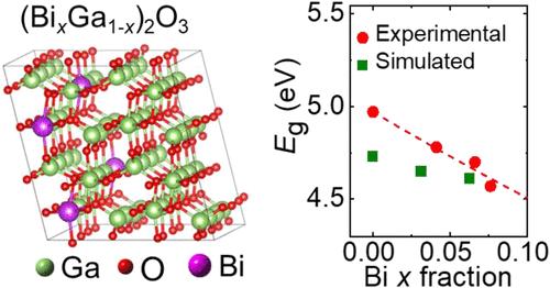
Bismuth (Bi) has recently emerged as a promising dopant for engineering the valence band of Ga2O3 to enable p-type doping. This study investigates the structural, electronic and optical effects of Bi incorporation in the ternary oxide (BixGa1–x)2O3 (x = 0 to 0.08) using a combination of experiments and density functional theory (DFT) calculations. Alloying Ga2O3 with Bi2O3 induces an upward shift of 0.37 eV in the valence band maximum (VBM) while preserving the monoclinic crystal structure. The band gap decreases from 4.97 to 4.57 eV, and the electrical conductivity of the (BixGa1–x)2O3 films reduces by over 2 orders of magnitude as the Bi fraction increases. This conductivity reduction is attributed to greater electron carrier compensation arising from the VBM upshift and a larger effective electron mass. Enhanced defect-related luminescence is observed in (BixGa1–x)2O3, in agreement with DFT calculations showing that the presence of nearby Bi atoms reduces the formation energy of Ga vacancies from 3.69 to 1.43 eV. These findings highlight the potential of Bi2O3 alloying for band structure engineering in Ga2O3 to facilitate p-type doping.
期刊介绍:
The Journal of Physical Chemistry A/B/C is devoted to reporting new and original experimental and theoretical basic research of interest to physical chemists, biophysical chemists, and chemical physicists.
 求助内容:
求助内容: 应助结果提醒方式:


