Yu. D. Filatov, A. Y. Boyarintsev, O. V. Kolesnikov, S. M. Galkin, V. O. Novgorodtsev, Ya. I. Polupan, O. I. Pylypenko, V. I. Sidorko, S. V. Kovalev
{"title":"Polishing of Optotechnical Parts Made of Semiconductor Materials","authors":"Yu. D. Filatov, A. Y. Boyarintsev, O. V. Kolesnikov, S. M. Galkin, V. O. Novgorodtsev, Ya. I. Polupan, O. I. Pylypenko, V. I. Sidorko, S. V. Kovalev","doi":"10.3103/S1063457625020029","DOIUrl":null,"url":null,"abstract":"<p>The study of the mechanism of material removal and particle wear in the dispersive phase of a dispersive system during semiconductor material polishing revealed that the formation of slurry nanoparticles and polishing powder wear nanoparticles results from QD-FRET, a Förster resonance energy transfer mediated by quantum materials. The energy transferred between polishing powder particles and the treated surface, as well as the energy of slurry nanoparticles and polishing powder wear nanoparticles, depend parabolically on their most probable sizes, which are interrelated with the effective width of the quantum material’s bandgap. The material removal rate and the intensity of polishing powder wear decrease exponentially as the effective bandgap width increases on the corresponding surfaces. Their ratio, which characterizes the efficiency of using a dispersive system of micro- and nanopowders for semiconductor material polishing, increases linearly with a decrease in the treated surface area and the surface area of polishing powder particles. The results of theoretical calculations of the material removal rate agree well with experimental data on the polishing performance of InSb, SiC, and Ge crystals, with a deviation of 4–5%.</p>","PeriodicalId":670,"journal":{"name":"Journal of Superhard Materials","volume":"47 2","pages":"125 - 136"},"PeriodicalIF":1.2000,"publicationDate":"2025-05-26","publicationTypes":"Journal Article","fieldsOfStudy":null,"isOpenAccess":false,"openAccessPdf":"","citationCount":"0","resultStr":null,"platform":"Semanticscholar","paperid":null,"PeriodicalName":"Journal of Superhard Materials","FirstCategoryId":"88","ListUrlMain":"https://link.springer.com/article/10.3103/S1063457625020029","RegionNum":4,"RegionCategory":"材料科学","ArticlePicture":[],"TitleCN":null,"AbstractTextCN":null,"PMCID":null,"EPubDate":"","PubModel":"","JCR":"Q4","JCRName":"MATERIALS SCIENCE, MULTIDISCIPLINARY","Score":null,"Total":0}
引用次数: 0
Abstract
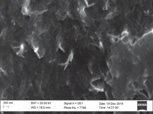
The study of the mechanism of material removal and particle wear in the dispersive phase of a dispersive system during semiconductor material polishing revealed that the formation of slurry nanoparticles and polishing powder wear nanoparticles results from QD-FRET, a Förster resonance energy transfer mediated by quantum materials. The energy transferred between polishing powder particles and the treated surface, as well as the energy of slurry nanoparticles and polishing powder wear nanoparticles, depend parabolically on their most probable sizes, which are interrelated with the effective width of the quantum material’s bandgap. The material removal rate and the intensity of polishing powder wear decrease exponentially as the effective bandgap width increases on the corresponding surfaces. Their ratio, which characterizes the efficiency of using a dispersive system of micro- and nanopowders for semiconductor material polishing, increases linearly with a decrease in the treated surface area and the surface area of polishing powder particles. The results of theoretical calculations of the material removal rate agree well with experimental data on the polishing performance of InSb, SiC, and Ge crystals, with a deviation of 4–5%.
期刊介绍:
Journal of Superhard Materials presents up-to-date results of basic and applied research on production, properties, and applications of superhard materials and related tools. It publishes the results of fundamental research on physicochemical processes of forming and growth of single-crystal, polycrystalline, and dispersed materials, diamond and diamond-like films; developments of methods for spontaneous and controlled synthesis of superhard materials and methods for static, explosive and epitaxial synthesis. The focus of the journal is large single crystals of synthetic diamonds; elite grinding powders and micron powders of synthetic diamonds and cubic boron nitride; polycrystalline and composite superhard materials based on diamond and cubic boron nitride; diamond and carbide tools for highly efficient metal-working, boring, stone-working, coal mining and geological exploration; articles of ceramic; polishing pastes for high-precision optics; precision lathes for diamond turning; technologies of precise machining of metals, glass, and ceramics. The journal covers all fundamental and technological aspects of synthesis, characterization, properties, devices and applications of these materials. The journal welcomes manuscripts from all countries in the English language.
 求助内容:
求助内容: 应助结果提醒方式:


