A bifunctional floral TiO2–TiB2 heterostructure buried interface on SnO2 for 23.5 % efficient n–i–p perovskite solar cells
IF 6.8
3区 材料科学
Q1 MATERIALS SCIENCE, MULTIDISCIPLINARY
Journal of Science: Advanced Materials and Devices
Pub Date : 2025-05-10
DOI:10.1016/j.jsamd.2025.100899
引用次数: 0
Abstract
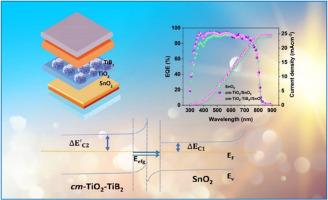
Interfacial energy mismatch and carrier recombination at the electron transport layer (ETL)/perovskite interface significantly limit the performance of perovskite solar cells (PSCs). We present a bifunctional dual-layer electron transport layer consisting of a floral TiO2–TiB2 heterostructure integrated on SnO2 to address these limitations. The TiO2–TiB2 heterostructure, formed through the partial oxidation of hydrothermally produced TiB2 nanoflakes, exhibits advantageous energy band alignment and provides a robust internal electric field at the buried interface, as confirmed by UPS, Mott–Schottky, and KPFM studies. This facilitates effective charge extraction, diminishes trap-assisted recombination, and improves perovskite crystallization while minimizing lattice strain. The optimized dual-layer ETL attains a power conversion efficiency (PCE) of 23.5 %, with a VOC of 1.201 V, J_SC of 24.5 mA cm−2, and a fill factor of 78.81 % in n–i–p structured perovskite solar cells utilizing α-FAPbI3. Improved charge carrier mobility and reduced trap density were validated by SCLC, TRPL, and EIS studies. The gadget demonstrates outstanding operational and environmental stability under heat, moisture, and prolonged light-stress conditions. This study presents a scalable approach for interfacial engineering of dual-layer electron transport layers to achieve extremely efficient and durable perovskite photovoltaics.
23.5%高效n-i-p钙钛矿太阳能电池在SnO2表面的双功能花状TiO2-TiB2异质结构埋藏界面
钙钛矿太阳能电池(PSCs)在电子传输层(ETL)/钙钛矿界面上的界面能量失配和载流子复合严重限制了电池的性能。我们提出了一种双功能的双层电子传输层,由花状TiO2-TiB2异质结构集成在SnO2上,以解决这些限制。UPS、Mott-Schottky和KPFM研究证实,通过水热生成的TiB2纳米片的部分氧化形成的TiO2-TiB2异质结构具有有利的能带对准,并在埋藏界面处提供强大的内部电场。这有利于有效的电荷提取,减少陷阱辅助复合,改善钙钛矿结晶,同时最小化晶格应变。优化后的双层ETL在n-i-p结构钙钛矿太阳能电池中获得了23.5%的功率转换效率(PCE), VOC为1.201 V, J_SC为24.5 mA cm−2,填充系数为78.81%。SCLC、TRPL和EIS研究证实了电荷载流子迁移率的提高和陷阱密度的降低。该装置在高温、潮湿和长时间光应力条件下表现出出色的操作和环境稳定性。本研究提出了一种可扩展的双层电子传输层界面工程方法,以实现极其高效和耐用的钙钛矿光伏发电。
本文章由计算机程序翻译,如有差异,请以英文原文为准。
求助全文
约1分钟内获得全文
求助全文
来源期刊
Journal of Science: Advanced Materials and Devices
Materials Science-Electronic, Optical and Magnetic Materials
CiteScore
11.90
自引率
2.50%
发文量
88
审稿时长
47 days
期刊介绍:
In 1985, the Journal of Science was founded as a platform for publishing national and international research papers across various disciplines, including natural sciences, technology, social sciences, and humanities. Over the years, the journal has experienced remarkable growth in terms of quality, size, and scope. Today, it encompasses a diverse range of publications dedicated to academic research.
Considering the rapid expansion of materials science, we are pleased to introduce the Journal of Science: Advanced Materials and Devices. This new addition to our journal series offers researchers an exciting opportunity to publish their work on all aspects of materials science and technology within the esteemed Journal of Science.
With this development, we aim to revolutionize the way research in materials science is expressed and organized, further strengthening our commitment to promoting outstanding research across various scientific and technological fields.
 求助内容:
求助内容: 应助结果提醒方式:


