Simulation on the Miniaturization and Performance Improvement Study of Gr/MoS2 Based Vertical Field Effect Transistor

IF 2.9 4区 工程技术 Q1 MULTIDISCIPLINARY SCIENCES
Sirsendu Ghosh, Anamika Devi Laishram, Pramod Kumar
{"title":"Simulation on the Miniaturization and Performance Improvement Study of Gr/MoS2 Based Vertical Field Effect Transistor","authors":"Sirsendu Ghosh, Anamika Devi Laishram, Pramod Kumar","doi":"10.1002/adts.202500139","DOIUrl":null,"url":null,"abstract":"Vertical field effect transistors (VFETs) show many advantages such as high switching speed, low operating voltage, low power consumption, and miniaturization over lateral FETs. Graphene (Gr) and transition metal di-chalcogenides (TMDs) are attractive 2D materials for the next generation electronics due to their subnanometer monolayer thickness. The layer by layer structure in 2D materials allows device fabrication down to a monolayer or a few layers, hence advantageous for VOFETs. In this simulation work, the bulk molybdenum disulfide (MoS<sub>2</sub>) is sandwiched between perforated monolayer graphene which acts as the source electrode, and aluminum (Al) as the top drain electrode. In addition to this, the minimization of the off-state current is carried out by modifications in the source contact geometry by insulating some part of the source electrode and introducing the extra MoS<sub>2</sub> layer between the source and gate dielectric named as buried layer. After the modification, the results show an improvement in OFF current, hence the ON/OFF ratio. The ON/OFF ratio of 10<sup>6</sup> is achieved for the device with a gate width and channel length of 100 nm. Additionally, the gate width is miniaturized to 50 nm by introducing insulation on the source contact to achieve similar performance.","PeriodicalId":7219,"journal":{"name":"Advanced Theory and Simulations","volume":"38 1","pages":""},"PeriodicalIF":2.9000,"publicationDate":"2025-05-06","publicationTypes":"Journal Article","fieldsOfStudy":null,"isOpenAccess":false,"openAccessPdf":"","citationCount":"0","resultStr":null,"platform":"Semanticscholar","paperid":null,"PeriodicalName":"Advanced Theory and Simulations","FirstCategoryId":"5","ListUrlMain":"https://doi.org/10.1002/adts.202500139","RegionNum":4,"RegionCategory":"工程技术","ArticlePicture":[],"TitleCN":null,"AbstractTextCN":null,"PMCID":null,"EPubDate":"","PubModel":"","JCR":"Q1","JCRName":"MULTIDISCIPLINARY SCIENCES","Score":null,"Total":0}
引用次数: 0

Abstract

Vertical field effect transistors (VFETs) show many advantages such as high switching speed, low operating voltage, low power consumption, and miniaturization over lateral FETs. Graphene (Gr) and transition metal di-chalcogenides (TMDs) are attractive 2D materials for the next generation electronics due to their subnanometer monolayer thickness. The layer by layer structure in 2D materials allows device fabrication down to a monolayer or a few layers, hence advantageous for VOFETs. In this simulation work, the bulk molybdenum disulfide (MoS2) is sandwiched between perforated monolayer graphene which acts as the source electrode, and aluminum (Al) as the top drain electrode. In addition to this, the minimization of the off-state current is carried out by modifications in the source contact geometry by insulating some part of the source electrode and introducing the extra MoS2 layer between the source and gate dielectric named as buried layer. After the modification, the results show an improvement in OFF current, hence the ON/OFF ratio. The ON/OFF ratio of 106 is achieved for the device with a gate width and channel length of 100 nm. Additionally, the gate width is miniaturized to 50 nm by introducing insulation on the source contact to achieve similar performance.

Abstract Image

Gr/MoS2垂直场效应晶体管小型化及性能提升仿真研究
垂直场效应晶体管(vfet)具有开关速度快、工作电压低、功耗低、小型化等优点。石墨烯(Gr)和过渡金属二硫族化合物(TMDs)由于其亚纳米单层厚度而成为下一代电子器件有吸引力的二维材料。二维材料中的逐层结构允许器件制造到单层或几层,因此对vofet有利。在这项模拟工作中,大块二硫化钼(MoS2)被夹在多孔单层石墨烯作为源电极和铝(Al)作为顶部漏极之间。除此之外,通过对源电极的某些部分进行绝缘,并在源和栅极介电介质之间引入额外的MoS2层(称为埋层),从而修改源接触几何形状,从而实现了断开状态电流的最小化。修改后,结果显示关闭电流的改善,因此开/关比。对于栅极宽度和通道长度为100 nm的器件,实现了106的开/关比。此外,通过在源触点上引入绝缘,栅极宽度缩小到50 nm,以实现类似的性能。
本文章由计算机程序翻译,如有差异,请以英文原文为准。
求助全文
约1分钟内获得全文 求助全文
来源期刊
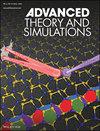
Advanced Theory and Simulations
Advanced Theory and Simulations Multidisciplinary-Multidisciplinary
CiteScore
5.50
自引率
3.00%
发文量
221
期刊介绍: Advanced Theory and Simulations is an interdisciplinary, international, English-language journal that publishes high-quality scientific results focusing on the development and application of theoretical methods, modeling and simulation approaches in all natural science and medicine areas, including: materials, chemistry, condensed matter physics engineering, energy life science, biology, medicine atmospheric/environmental science, climate science planetary science, astronomy, cosmology method development, numerical methods, statistics
×
引用
GB/T 7714-2015
复制
MLA
复制
APA
复制
导出至
BibTeX EndNote RefMan NoteFirst NoteExpress
×
提示
您的信息不完整,为了账户安全,请先补充。
现在去补充
×
提示
您因"违规操作"
具体请查看互助需知
我知道了
×
提示
确定
请完成安全验证×
copy
已复制链接
快去分享给好友吧!
我知道了
右上角分享
点击右上角分享
0
联系我们:info@booksci.cn Book学术提供免费学术资源搜索服务,方便国内外学者检索中英文文献。致力于提供最便捷和优质的服务体验。 Copyright © 2023 布克学术 All rights reserved.
京ICP备2023020795号-1
ghs 京公网安备 11010802042870号
Book学术文献互助
Book学术文献互助群
群 号:604180095
Book学术官方微信