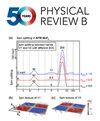
Tanay Tak, Wan Ying Ho, Iris Celupica-Liu, Yi Chao Chow, Jacques Peretti, Claude Weisbuch, James S. Speck
{"title":"Trap-assisted Auger-Meitner recombination in GaN p-i-n diodes","authors":"Tanay Tak, Wan Ying Ho, Iris Celupica-Liu, Yi Chao Chow, Jacques Peretti, Claude Weisbuch, James S. Speck","doi":"10.1103/physrevb.111.155308","DOIUrl":null,"url":null,"abstract":"Most properties of semiconductor devices are dominated by shallow impurities. However, deep defects often play an important role, for instance, in recombination processes or high field transport. While a variety of techniques are available to assess the density and energy levels of impurities, other properties, such as the recombination mechanisms of the defects, escape observation. We report on the direct measurement of hot electrons generated by trap-assisted Auger-Meitner recombination (TAAR) in GaN diodes. By performing electron emission spectroscopy (EES) on diodes with surfaces activated to negative electron affinity by cesium, we observe the expected overflow electrons of diodes under low current injection. However, when operating the devices at higher current densities, as low as ∼25 A/c</a:mi>m</a:mi></a:mrow>2</a:mn></a:msup></a:mrow></a:math>, we measure the emission of high-energy electrons. At variance with the observed hot electrons in light-emitting diodes (LEDs) using EES, the hot electrons generated in diodes at our tested currents cannot be from Auger-Meitner recombination due to the diodes' significantly lower carrier densities compared to those in LEDs. During our measurements, we observe the emission of accumulated electrons with energies ∼0.42 eV, ∼0.99 eV, ∼1.43 eV, and ∼2.32 eV above the conduction-band minimum (CBM) at various bias conditions, suggesting the existence of conduction-band features in GaN at these energies where electrons can be long-lived, such as satellite-valley minima and inflection points. We also measure incompletely relaxed hot electrons approaching energies 1.97 ± 0.13 eV and 2.94 ± 0.13 eV above the CBM, as the diodes are biased to high currents, suggesting at least some of the TAAR partaking defects have an energy level <d:math xmlns:d=\"http://www.w3.org/1998/Math/MathML\"><d:mo>≳</d:mo><d:mn>1.97</d:mn></d:math> eV and <e:math xmlns:e=\"http://www.w3.org/1998/Math/MathML\"><e:mo>≳</e:mo><e:mn>2.94</e:mn></e:math> eV away from either the conduction or valence band edges. Additionally, at our highest operating currents, we measure hot electrons with energies 3.28 ± 0.13 eV above the CBM, providing direct evidence of TAAR processes involving shallow impurities. This unexpected observation of TAAR in GaN diodes spotlights the importance of further studies of defects in GaN and the necessity to incorporate the multi-phonon emission, radiative, and TAAR capture steps of defect-assisted recombination cycles into device modeling. Furthermore, this experiment demonstrates the applicability of the simplest semiconductor structures, diodes, as a test bed to study the rich recombination physics of semiconductor materials. <jats:supplementary-material> <jats:copyright-statement>Published by the American Physical Society</jats:copyright-statement> <jats:copyright-year>2025</jats:copyright-year> </jats:permissions> </jats:supplementary-material>","PeriodicalId":20082,"journal":{"name":"Physical Review B","volume":"7 1","pages":""},"PeriodicalIF":3.7000,"publicationDate":"2025-05-01","publicationTypes":"Journal Article","fieldsOfStudy":null,"isOpenAccess":false,"openAccessPdf":"","citationCount":"0","resultStr":null,"platform":"Semanticscholar","paperid":null,"PeriodicalName":"Physical Review B","FirstCategoryId":"101","ListUrlMain":"https://doi.org/10.1103/physrevb.111.155308","RegionNum":2,"RegionCategory":"物理与天体物理","ArticlePicture":[],"TitleCN":null,"AbstractTextCN":null,"PMCID":null,"EPubDate":"","PubModel":"","JCR":"Q1","JCRName":"Physics and Astronomy","Score":null,"Total":0}
引用次数: 0
Abstract
Most properties of semiconductor devices are dominated by shallow impurities. However, deep defects often play an important role, for instance, in recombination processes or high field transport. While a variety of techniques are available to assess the density and energy levels of impurities, other properties, such as the recombination mechanisms of the defects, escape observation. We report on the direct measurement of hot electrons generated by trap-assisted Auger-Meitner recombination (TAAR) in GaN diodes. By performing electron emission spectroscopy (EES) on diodes with surfaces activated to negative electron affinity by cesium, we observe the expected overflow electrons of diodes under low current injection. However, when operating the devices at higher current densities, as low as ∼25 A/cm2, we measure the emission of high-energy electrons. At variance with the observed hot electrons in light-emitting diodes (LEDs) using EES, the hot electrons generated in diodes at our tested currents cannot be from Auger-Meitner recombination due to the diodes' significantly lower carrier densities compared to those in LEDs. During our measurements, we observe the emission of accumulated electrons with energies ∼0.42 eV, ∼0.99 eV, ∼1.43 eV, and ∼2.32 eV above the conduction-band minimum (CBM) at various bias conditions, suggesting the existence of conduction-band features in GaN at these energies where electrons can be long-lived, such as satellite-valley minima and inflection points. We also measure incompletely relaxed hot electrons approaching energies 1.97 ± 0.13 eV and 2.94 ± 0.13 eV above the CBM, as the diodes are biased to high currents, suggesting at least some of the TAAR partaking defects have an energy level ≳1.97 eV and ≳2.94 eV away from either the conduction or valence band edges. Additionally, at our highest operating currents, we measure hot electrons with energies 3.28 ± 0.13 eV above the CBM, providing direct evidence of TAAR processes involving shallow impurities. This unexpected observation of TAAR in GaN diodes spotlights the importance of further studies of defects in GaN and the necessity to incorporate the multi-phonon emission, radiative, and TAAR capture steps of defect-assisted recombination cycles into device modeling. Furthermore, this experiment demonstrates the applicability of the simplest semiconductor structures, diodes, as a test bed to study the rich recombination physics of semiconductor materials. Published by the American Physical Society2025
期刊介绍:
Physical Review B (PRB) is the world’s largest dedicated physics journal, publishing approximately 100 new, high-quality papers each week. The most highly cited journal in condensed matter physics, PRB provides outstanding depth and breadth of coverage, combined with unrivaled context and background for ongoing research by scientists worldwide.
PRB covers the full range of condensed matter, materials physics, and related subfields, including:
-Structure and phase transitions
-Ferroelectrics and multiferroics
-Disordered systems and alloys
-Magnetism
-Superconductivity
-Electronic structure, photonics, and metamaterials
-Semiconductors and mesoscopic systems
-Surfaces, nanoscience, and two-dimensional materials
-Topological states of matter