Modeling and Simulation of AlPN/GaN High Electron Mobility Transistor
IF 2.9
4区 工程技术
Q1 MULTIDISCIPLINARY SCIENCES
引用次数: 0
Abstract
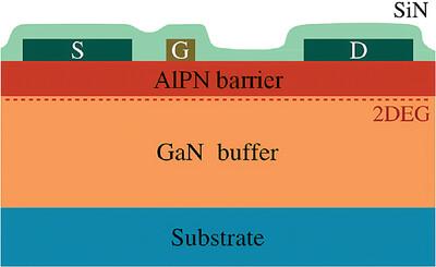
AlPN is a relatively new semiconductor alloy capable of providing high two‐dimensional electron gas Two‐Dimensional Electron Gas (2DEG) densities on the order of 1013 cm
AlPN/GaN高电子迁移率晶体管的建模与仿真
AlPN是一种相对较新的半导体合金,能够在与GaN的异质结界面上提供高达1013 cm−2的二维电子气体(2DEG)密度。磷的摩尔分数可以调节,以实现晶格匹配的AlPN/GaN异质结,具有很强的自发极化。因此,与AlGaN/GaN异质结相比,这在界面处诱导出更多的电子,导致更低的片电阻,使AlPN成为高电子迁移率晶体管(hemt)的最佳势垒。在这项工作中,模拟了AlPN/GaN HEMT,并与相应的AlGaN/GaN HEMT进行了比较。AlPN/GaN HEMT的最大漏极电流密度为1.85 a /mm,是AlGaN/GaN HEMT的两倍,使该器件能够在高频下实现更高的功率密度。AlPN/GaN HEMT的峰值跨导率为0.293 S/mm,是AlGaN/GaN HEMT的三倍以上,可以用于传感器应用,因为HEMT的灵敏度与跨导率成正比。此外,AlPN/GaN HEMT获得了比AlGaN/GaN HEMT更低的噪声系数,这对于低噪声放大器设计至关重要。因此,改进AlPN器件的制备和生长技术有利于稳定生产。
本文章由计算机程序翻译,如有差异,请以英文原文为准。
求助全文
约1分钟内获得全文
求助全文
来源期刊
Advanced Theory and Simulations
Multidisciplinary-Multidisciplinary
CiteScore
5.50
自引率
3.00%
发文量
221
期刊介绍:
Advanced Theory and Simulations is an interdisciplinary, international, English-language journal that publishes high-quality scientific results focusing on the development and application of theoretical methods, modeling and simulation approaches in all natural science and medicine areas, including:
materials, chemistry, condensed matter physics
engineering, energy
life science, biology, medicine
atmospheric/environmental science, climate science
planetary science, astronomy, cosmology
method development, numerical methods, statistics
 求助内容:
求助内容: 应助结果提醒方式:


