Oxidation Temperature-Dependent Electrochemical Doping of WO3 Deposited via Atomic Layer Deposition

IF 3.3 3区 化学 Q2 CHEMISTRY, PHYSICAL
Alexandria R. C. Bredar, Hannah R. M. Margavio, Carrie Donley, Neil Spinner, Nyaan Amin, Gregory N. Parsons, Jillian L. Dempsey
{"title":"Oxidation Temperature-Dependent Electrochemical Doping of WO3 Deposited via Atomic Layer Deposition","authors":"Alexandria R. C. Bredar, Hannah R. M. Margavio, Carrie Donley, Neil Spinner, Nyaan Amin, Gregory N. Parsons, Jillian L. Dempsey","doi":"10.1021/acs.jpcc.4c06105","DOIUrl":null,"url":null,"abstract":"Silicon-based photoelectrochemical devices show promise for the performance of light-driven CO<sub>2</sub> reduction but suffer from instability under photoelectrochemical conditions relevant to CO<sub>2</sub> reduction. Coating silicon electrodes with thin layers of metal oxides has shown promise to passivate unstable silicon surfaces, and many different metal oxides can be deposited on silicon using various techniques. In this study, we investigate the fundamental photoelectrochemical performance of WO<sub>3</sub>-coated silicon photoelectrodes, which were generated by oxidation of W-metal films deposited via atomic layer deposition on both degenerately doped (nSi<sup>+</sup>) and low-doped (pSi) silicon. Two different oxidation temperatures were investigated (400 and 600 °C), and it was found that the monoclinic phase of WO<sub>3</sub> predominates at both temperatures but that more grain boundaries are present in the 600 °C film. From X-ray photoelectron spectroscopy, the stoichiometry of both films was found to be 1:3 W:O, and low electron energy loss experiments indicate band gaps of 3.0 and 3.1 eV for 400 and 600 °C films, respectively. Cyclic voltammetry experiments showed that the electron transfer kinetics increased after continued redox cycling, particularly for the material produced at 400 °C. X-ray photoelectron spectra suggest that the observed increase in electrode conductivity is due to the formation of oxygen vacancies in the film. Electrochemical impedance spectroscopy indicated that charge transport through the films was impacted by the grain boundaries that formed during oxidation of the film. Photoelectrochemical studies on pSi/WO<sub>3</sub> electrodes were highly variable, only producing a photocurrent and photovoltage with some samples. Our best sample, formed at 400 °C, produced a photovoltage of 180 mV, which is lower than what has previously been reported for WO<sub>3</sub>-coated silicon (500 mV). We hypothesize that the variability in photoelectrochemical experiments arose from a roughened WSiO<sub><i>x</i></sub> interface that is generated during film preparation. WO<sub>3</sub> shows promise as a metal oxide coating for silicon, but our results suggest that formation of a high-quality interface between Si and WO<sub>3</sub> is vital for best performance.","PeriodicalId":61,"journal":{"name":"The Journal of Physical Chemistry C","volume":"83 1","pages":""},"PeriodicalIF":3.3000,"publicationDate":"2024-12-09","publicationTypes":"Journal Article","fieldsOfStudy":null,"isOpenAccess":false,"openAccessPdf":"","citationCount":"0","resultStr":null,"platform":"Semanticscholar","paperid":null,"PeriodicalName":"The Journal of Physical Chemistry C","FirstCategoryId":"1","ListUrlMain":"https://doi.org/10.1021/acs.jpcc.4c06105","RegionNum":3,"RegionCategory":"化学","ArticlePicture":[],"TitleCN":null,"AbstractTextCN":null,"PMCID":null,"EPubDate":"","PubModel":"","JCR":"Q2","JCRName":"CHEMISTRY, PHYSICAL","Score":null,"Total":0}
引用次数: 0

Abstract

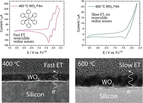
Silicon-based photoelectrochemical devices show promise for the performance of light-driven CO2 reduction but suffer from instability under photoelectrochemical conditions relevant to CO2 reduction. Coating silicon electrodes with thin layers of metal oxides has shown promise to passivate unstable silicon surfaces, and many different metal oxides can be deposited on silicon using various techniques. In this study, we investigate the fundamental photoelectrochemical performance of WO3-coated silicon photoelectrodes, which were generated by oxidation of W-metal films deposited via atomic layer deposition on both degenerately doped (nSi+) and low-doped (pSi) silicon. Two different oxidation temperatures were investigated (400 and 600 °C), and it was found that the monoclinic phase of WO3 predominates at both temperatures but that more grain boundaries are present in the 600 °C film. From X-ray photoelectron spectroscopy, the stoichiometry of both films was found to be 1:3 W:O, and low electron energy loss experiments indicate band gaps of 3.0 and 3.1 eV for 400 and 600 °C films, respectively. Cyclic voltammetry experiments showed that the electron transfer kinetics increased after continued redox cycling, particularly for the material produced at 400 °C. X-ray photoelectron spectra suggest that the observed increase in electrode conductivity is due to the formation of oxygen vacancies in the film. Electrochemical impedance spectroscopy indicated that charge transport through the films was impacted by the grain boundaries that formed during oxidation of the film. Photoelectrochemical studies on pSi/WO3 electrodes were highly variable, only producing a photocurrent and photovoltage with some samples. Our best sample, formed at 400 °C, produced a photovoltage of 180 mV, which is lower than what has previously been reported for WO3-coated silicon (500 mV). We hypothesize that the variability in photoelectrochemical experiments arose from a roughened WSiOx interface that is generated during film preparation. WO3 shows promise as a metal oxide coating for silicon, but our results suggest that formation of a high-quality interface between Si and WO3 is vital for best performance.

Abstract Image

原子层沉积WO3的氧化温度依赖性电化学掺杂
硅基光电化学器件在光驱动CO2还原方面表现出良好的性能,但在与CO2还原相关的光电化学条件下存在不稳定性。在硅电极上涂上薄层金属氧化物有望钝化不稳定的硅表面,并且可以使用各种技术将许多不同的金属氧化物沉积在硅上。在本研究中,我们研究了wo3包覆硅光电极的基本光电电化学性能,该电极是通过原子层沉积在简并掺杂(nSi+)和低掺杂(pSi)硅上的w金属膜氧化而产生的。在400℃和600℃两种不同的氧化温度下,WO3均以单斜相为主,但在600℃的氧化膜中存在较多的晶界。通过x射线光电子能谱分析,发现两种薄膜的化学计量为1:3 W:O,低电子能量损失实验表明,400°C和600°C薄膜的带隙分别为3.0和3.1 eV。循环伏安法实验表明,继续氧化还原循环后,电子传递动力学增加,特别是在400°C下产生的材料。x射线光电子能谱表明,所观察到的电极电导率的增加是由于在薄膜中形成氧空位。电化学阻抗谱分析表明,薄膜氧化过程中形成的晶界影响了电荷在薄膜中的输运。在pSi/WO3电极上的光电化学研究变化很大,在某些样品上只能产生光电流和光电压。我们的最佳样品在400°C下形成,产生180 mV的光电压,这比之前报道的wo3涂层硅(500 mV)的光电压低。我们假设,光电化学实验中的变异性是由薄膜制备过程中产生的粗糙的WSiOx界面引起的。WO3有望作为硅的金属氧化物涂层,但我们的研究结果表明,在Si和WO3之间形成高质量的界面对于获得最佳性能至关重要。
本文章由计算机程序翻译,如有差异,请以英文原文为准。
求助全文
约1分钟内获得全文 求助全文
来源期刊
The Journal of Physical Chemistry C
The Journal of Physical Chemistry C 化学-材料科学:综合
CiteScore
6.50
自引率
8.10%
发文量
2047
审稿时长
1.8 months
期刊介绍: The Journal of Physical Chemistry A/B/C is devoted to reporting new and original experimental and theoretical basic research of interest to physical chemists, biophysical chemists, and chemical physicists.
×
引用
GB/T 7714-2015
复制
MLA
复制
APA
复制
导出至
BibTeX EndNote RefMan NoteFirst NoteExpress
×
提示
您的信息不完整,为了账户安全,请先补充。
现在去补充
×
提示
您因"违规操作"
具体请查看互助需知
我知道了
×
提示
确定
请完成安全验证×
copy
已复制链接
快去分享给好友吧!
我知道了
右上角分享
点击右上角分享
0
联系我们:info@booksci.cn Book学术提供免费学术资源搜索服务,方便国内外学者检索中英文文献。致力于提供最便捷和优质的服务体验。 Copyright © 2023 布克学术 All rights reserved.
京ICP备2023020795号-1
ghs 京公网安备 11010802042870号
Book学术文献互助
Book学术文献互助群
群 号:481959085
Book学术官方微信