Surface evolution mechanism for atomic-scale smoothing of Si via atmospheric pressure plasma etching

IF 6.1 1区 工程技术 Q1 ENGINEERING, MANUFACTURING
Bing Wu , Rong Yi , Xuemiao Ding , Tom Chiu , Quanpeng He , Hui Deng
{"title":"Surface evolution mechanism for atomic-scale smoothing of Si via atmospheric pressure plasma etching","authors":"Bing Wu ,&nbsp;Rong Yi ,&nbsp;Xuemiao Ding ,&nbsp;Tom Chiu ,&nbsp;Quanpeng He ,&nbsp;Hui Deng","doi":"10.1016/j.jmapro.2024.10.080","DOIUrl":null,"url":null,"abstract":"<div><div>Atmospheric plasma etching-based machining methods generally suffer from surface roughness deterioration. To achieve an atomic-scale smooth surface of Si via purely plasma etching, clarifying the etching evolution and mechanism is essential. In this study, we study surface evolution and smoothening mechanisms from the perspective of plasma etching modes comprehensively. The morphology and roughness evolutions of isotropic, orientation-selective, and atom-selective etching are investigated, respectively. The semi-finishing effect is realized through the growing and merging of hemispherical pits during isotropic etching, with the surface roughness being reduced from 103 nm to 0.79 nm. Orientation-selective etching is a roughening process, transforming square-opening pits into pyramid structures. Under the atom-selective mode, an atomically smooth surface with <em>S</em>a 0.17 nm can be obtained. The top-down smoothing process of atom-selective is much more efficient than isotropic etching. Atom-selective etching with a maximum removal rate of 22 μm/min enables the rapid thinning of Si substrate thickness from 715 μm to 90.4 μm within 45 min. Additionally, atom-selective etching is a universal polishing approach regardless of pre-processed methods and is a damage-less process. This paper provides a promising strategy for atomic and close-to-atomic scale manufacturing.</div></div>","PeriodicalId":16148,"journal":{"name":"Journal of Manufacturing Processes","volume":"132 ","pages":"Pages 353-362"},"PeriodicalIF":6.1000,"publicationDate":"2024-11-06","publicationTypes":"Journal Article","fieldsOfStudy":null,"isOpenAccess":false,"openAccessPdf":"","citationCount":"0","resultStr":null,"platform":"Semanticscholar","paperid":null,"PeriodicalName":"Journal of Manufacturing Processes","FirstCategoryId":"5","ListUrlMain":"https://www.sciencedirect.com/science/article/pii/S1526612524011228","RegionNum":1,"RegionCategory":"工程技术","ArticlePicture":[],"TitleCN":null,"AbstractTextCN":null,"PMCID":null,"EPubDate":"","PubModel":"","JCR":"Q1","JCRName":"ENGINEERING, MANUFACTURING","Score":null,"Total":0}
引用次数: 0

Abstract

Atmospheric plasma etching-based machining methods generally suffer from surface roughness deterioration. To achieve an atomic-scale smooth surface of Si via purely plasma etching, clarifying the etching evolution and mechanism is essential. In this study, we study surface evolution and smoothening mechanisms from the perspective of plasma etching modes comprehensively. The morphology and roughness evolutions of isotropic, orientation-selective, and atom-selective etching are investigated, respectively. The semi-finishing effect is realized through the growing and merging of hemispherical pits during isotropic etching, with the surface roughness being reduced from 103 nm to 0.79 nm. Orientation-selective etching is a roughening process, transforming square-opening pits into pyramid structures. Under the atom-selective mode, an atomically smooth surface with Sa 0.17 nm can be obtained. The top-down smoothing process of atom-selective is much more efficient than isotropic etching. Atom-selective etching with a maximum removal rate of 22 μm/min enables the rapid thinning of Si substrate thickness from 715 μm to 90.4 μm within 45 min. Additionally, atom-selective etching is a universal polishing approach regardless of pre-processed methods and is a damage-less process. This paper provides a promising strategy for atomic and close-to-atomic scale manufacturing.
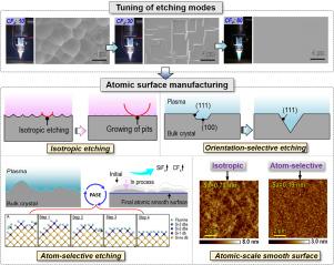
Abstract Image

通过常压等离子体蚀刻实现硅原子尺度平滑的表面演化机制
基于大气等离子体蚀刻的加工方法普遍存在表面粗糙度下降的问题。要想通过纯等离子体刻蚀获得原子尺度的平滑硅表面,必须弄清刻蚀的演变过程和机理。在本研究中,我们从等离子体刻蚀模式的角度全面研究了表面演化和光滑化机制。分别研究了各向同性蚀刻、取向选择性蚀刻和原子选择性蚀刻的形貌和粗糙度演变。在各向同性蚀刻过程中,通过半球形凹坑的生长和合并实现了半精加工效应,表面粗糙度从 103 nm 降低到 0.79 nm。方向选择性蚀刻是一种粗化过程,将方形开孔凹坑转化为金字塔结构。在原子选择模式下,可获得 Sa 值为 0.17 nm 的原子平滑表面。原子选择性自上而下的平滑过程比各向同性蚀刻更有效。原子选择性蚀刻的最大去除率为 22 μm/min,可在 45 分钟内将硅衬底厚度从 715 μm 快速减薄至 90.4 μm。此外,原子选择性蚀刻是一种通用的抛光方法,不受预处理方法的限制,而且是一种无损伤工艺。本文为原子级和近原子级制造提供了一种前景广阔的策略。
本文章由计算机程序翻译,如有差异,请以英文原文为准。
求助全文
约1分钟内获得全文 求助全文
来源期刊
Journal of Manufacturing Processes
Journal of Manufacturing Processes ENGINEERING, MANUFACTURING-
CiteScore
10.20
自引率
11.30%
发文量
833
审稿时长
50 days
期刊介绍: The aim of the Journal of Manufacturing Processes (JMP) is to exchange current and future directions of manufacturing processes research, development and implementation, and to publish archival scholarly literature with a view to advancing state-of-the-art manufacturing processes and encouraging innovation for developing new and efficient processes. The journal will also publish from other research communities for rapid communication of innovative new concepts. Special-topic issues on emerging technologies and invited papers will also be published.
×
引用
GB/T 7714-2015
复制
MLA
复制
APA
复制
导出至
BibTeX EndNote RefMan NoteFirst NoteExpress
×
提示
您的信息不完整,为了账户安全,请先补充。
现在去补充
×
提示
您因"违规操作"
具体请查看互助需知
我知道了
×
提示
确定
请完成安全验证×
copy
已复制链接
快去分享给好友吧!
我知道了
右上角分享
点击右上角分享
0
联系我们:info@booksci.cn Book学术提供免费学术资源搜索服务,方便国内外学者检索中英文文献。致力于提供最便捷和优质的服务体验。 Copyright © 2023 布克学术 All rights reserved.
京ICP备2023020795号-1
ghs 京公网安备 11010802042870号
Book学术文献互助
Book学术文献互助群
群 号:481959085
Book学术官方微信