The role of interface trap charges in MoS2 thickness engineered TFET
IF 3.1
3区 材料科学
Q2 MATERIALS SCIENCE, MULTIDISCIPLINARY
引用次数: 0
Abstract
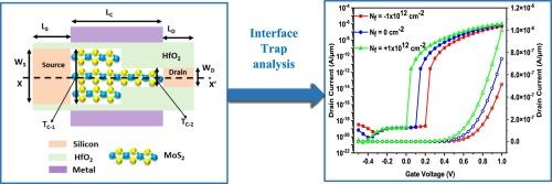
The 2D molybdenum disulfide (MoS2) based short-channel FET has shown remarkable performance, and there is an increasing demand for research on the factors that affect the device characteristics. Although interface trap charges (ITCs) have been observed during various experimental studies on MoS2-oxide interfaces, it is still unclear how this is affecting device-level performance. To fill this gap, the present work focuses on the impact of ITCs in MoS2 Thickness Engineered TFETs (MoS2 TE-TFET) by considering both positive (donor) and negative (acceptor) types of ITCs at the MoS2-HfO2 interface. The different ITC density ranges, such as Nf = −4 × 1012cm−2 to +4 × 1012 cm−2 and Nf = −4 × 1011cm−2 to +4 × 1011cm−2 are considered to explore ION, Vth, IOFF, ION/IOFF, transfer characteristics, energy band diagram, electric field, potential and maximum electron mobility device parameters. Additionally, a comparison of the ION/IOFF ratio, Vth, and electron mobility with existing literature is presented.

界面陷阱电荷在 MoS2 厚度工程 TFET 中的作用
基于二维二硫化钼(MoS2)的短沟道场效应晶体管已显示出非凡的性能,因此对影响器件特性的因素的研究需求日益增加。虽然在对 MoS2-氧化物界面进行的各种实验研究中已经观察到了界面陷阱电荷(ITC),但目前仍不清楚它是如何影响器件级性能的。为了填补这一空白,本研究通过考虑 MoS2-HfO2 界面正(供体)和负(受体)两种类型的 ITC,重点研究了 ITC 对 MoS2 厚度工程 TFET(MoS2 TE-TFET)的影响。考虑了不同的 ITC 密度范围,如 Nf = -4 × 1012cm-2 至 +4 × 1012cm-2 和 Nf = -4 × 1011cm-2 至 +4 × 1011cm-2,以探索 ION、Vth、IOFF、ION/IOFF、转移特性、能带图、电场、电势和最大电子迁移率等器件参数。此外,还对 ION/IOFF 比率、Vth 和电子迁移率与现有文献进行了比较。
本文章由计算机程序翻译,如有差异,请以英文原文为准。
求助全文
约1分钟内获得全文
求助全文
来源期刊

Computational Materials Science
工程技术-材料科学:综合
CiteScore
6.50
自引率
6.10%
发文量
665
审稿时长
26 days
期刊介绍:
The goal of Computational Materials Science is to report on results that provide new or unique insights into, or significantly expand our understanding of, the properties of materials or phenomena associated with their design, synthesis, processing, characterization, and utilization. To be relevant to the journal, the results should be applied or applicable to specific material systems that are discussed within the submission.
 求助内容:
求助内容: 应助结果提醒方式:


