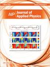
Strain engineering in 2D FETs: Physics, status, and prospects
IF 2.5
3区 物理与天体物理
Q2 PHYSICS, APPLIED
引用次数: 0
Abstract
In this work, we explore the physics and evaluate the merits of strain engineering in two-dimensional van der Waals semiconductor-based FETs (field-effect-transistors) using DFT (density functional theory) to determine the modulation of the channel material properties under strain, and subsequently, their effect on carrier transport properties, i.e., scattering rates, mobility, and then finally simulate and analyze dissipative current transport with a non-equilibrium Green's function–Poisson's equation self-consistent solver. The scattering model includes the effects of charged impurities, intrinsic phonons, and remote phonons as well as the screening effect due to charged carriers. Impact of strain engineering on contact resistance is also incorporated into the transport simulations to determine the potential performance enhancements using strain in practical devices. Based on the comprehensive simulation results, we identify the materials and strain configuration that provide the best improvement in performance. We demonstrate an ON-current gain of 43.3% in a biaxially compressively strained monolayer MoSe2 device achieved through unique valley-crossing. Furthermore, implications of strain engineering for emerging energy-efficient devices based on band-to-band tunneling and spintronics are evaluated to explore uncharted frontiers in beyond-CMOS electron devices.二维场效应晶体管中的应变工程:物理学、现状和前景
在这项研究中,我们利用 DFT(密度泛函理论)探讨了二维范德瓦尔斯半导体场效应晶体管(FET)的物理特性并评估了应变工程的优点,确定了应变下沟道材料特性的调制,以及随后它们对载流子传输特性(即散射率、迁移率)的影响,最后利用非平衡格林函数-泊松方程自洽求解器模拟和分析了耗散电流传输。散射模型包括带电杂质、本征声子、远程声子以及带电载流子的屏蔽效应。应变工程对接触电阻的影响也被纳入了传输模拟,以确定在实际器件中利用应变提高性能的潜力。根据全面的模拟结果,我们确定了能提供最佳性能改进的材料和应变配置。我们展示了在双轴压缩应变单层 MoSe2 器件中,通过独特的谷交叉实现了 43.3% 的导通电流增益。此外,我们还评估了应变工程对基于带对带隧道和自旋电子学的新兴高能效器件的影响,以探索超越 CMOS 电子器件的未知前沿。
本文章由计算机程序翻译,如有差异,请以英文原文为准。
求助全文
约1分钟内获得全文
求助全文
来源期刊

Journal of Applied Physics
物理-物理:应用
CiteScore
5.40
自引率
9.40%
发文量
1534
审稿时长
2.3 months
期刊介绍:
The Journal of Applied Physics (JAP) is an influential international journal publishing significant new experimental and theoretical results of applied physics research.
Topics covered in JAP are diverse and reflect the most current applied physics research, including:
Dielectrics, ferroelectrics, and multiferroics-
Electrical discharges, plasmas, and plasma-surface interactions-
Emerging, interdisciplinary, and other fields of applied physics-
Magnetism, spintronics, and superconductivity-
Organic-Inorganic systems, including organic electronics-
Photonics, plasmonics, photovoltaics, lasers, optical materials, and phenomena-
Physics of devices and sensors-
Physics of materials, including electrical, thermal, mechanical and other properties-
Physics of matter under extreme conditions-
Physics of nanoscale and low-dimensional systems, including atomic and quantum phenomena-
Physics of semiconductors-
Soft matter, fluids, and biophysics-
Thin films, interfaces, and surfaces
 求助内容:
求助内容: 应助结果提醒方式:


