Precise Patterning of Flexible Transparent and Conductive Films without Chemical Etchings and Applications in Capacitive Proximity Sensors
引用次数: 0
Abstract
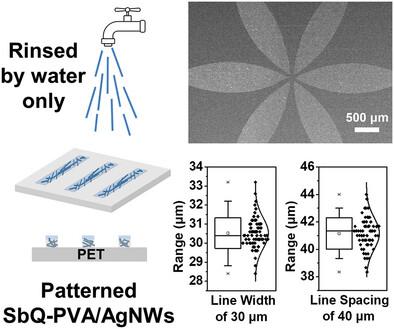
Process microminiaturization is in need not only in chip field, but also in sensor‐related industries. Touch panel sensors as an example have their man‐machine interactive performance in high relation with the circuit resolution. Traditional etchings by yellow light or laser encounter their resolution limit of ≈50 µm; moreover, former pollution using chemical etchants and latter damage to flexible substrates are inevitable. This paper demonstrates an efficient and green patterning technology for flexible silver nanowire (AgNW) transparent and conductive films, which can enable complicated patterns on various types of substrates with high resolution of a 30 µm line width and 40 µm line spacing. The approach uses a water‐soluble photosensitive polymer as the selective protection layer to facilitate the removal of unwanted AgNWs through simple water washing. Due to its good water resistance and mechanical properties, the patterned electrodes exhibit excellent flexibility and environmental stability. As a proof of concept, a capacitive proximity sensor is designed using the patterned AgNW electrodes of the micro feature size, which exhibits excellent proximity sensing performance. The developed patterning technology paves the way to miniaturized feature sizes of different optoelectronic devices for wide applications in fields like new‐style displays, man‐machine interaction, IoT sensing and intelligent robots.
无需化学蚀刻的柔性透明导电薄膜的精确图案化及其在电容式接近传感器中的应用
工艺微小型化不仅是芯片领域的需要,也是传感器相关行业的需要。例如,触摸屏传感器的人机交互性能与电路分辨率密切相关。传统的黄光蚀刻或激光蚀刻的分辨率极限在 50 微米以下;此外,前者使用化学蚀刻剂会造成污染,后者则不可避免地会损坏柔性基板。本文展示了一种高效、绿色的柔性银纳米线(AgNW)透明导电薄膜图案技术,它能在各种类型的基底上绘制复杂的图案,并具有 30 微米线宽和 40 微米线距的高分辨率。该方法使用水溶性光敏聚合物作为选择性保护层,便于通过简单的水洗去除不需要的 AgNW。由于其良好的耐水性和机械性能,图案化电极具有出色的柔韧性和环境稳定性。作为概念验证,使用微特征尺寸的图案化 AgNW 电极设计了一种电容式接近传感器,该传感器具有出色的接近感应性能。所开发的图案化技术为实现不同光电器件特征尺寸的微型化铺平了道路,可广泛应用于新型显示器、人机交互、物联网传感和智能机器人等领域。
本文章由计算机程序翻译,如有差异,请以英文原文为准。
求助全文
约1分钟内获得全文
求助全文

 求助内容:
求助内容: 应助结果提醒方式:


