Direct Reconstruction of the Band Diagram of Rhombohedral-Stacked Bilayer WSe2–Graphene Heterostructure via Photoemission Electron Microscopy
IF 5.4
3区 材料科学
Q2 CHEMISTRY, PHYSICAL
引用次数: 0
Abstract
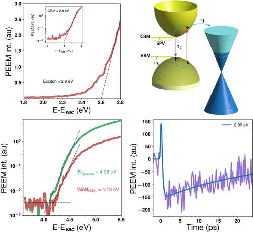
The determination of energy levels at heterointerfaces is important for understanding charge transport mechanisms, enabling judicious assembly of various electronic and optoelectronic devices. Herein, we investigated the interface properties of a heterostructure consisting of two-dimensional (2D) transition-metal dichalcogenides rhombohedral 3R (AB stacking) bilayer WSe2 (3R-2 ML WSe2) and epitaxial graphene using photoemission electron microscopy (PEEM) with a femtosecond laser excitation source. The 2D energy band diagram was imaged in an energy-resolved mode (ER-PEEM). For the 3R-2 ML WSe2, the conduction band minimum and the exciton were located at 2.0 and 2.6 eV, respectively, while the valence band maximum was at 4.18 eV. The Fermi level of graphene was located at 4.08 eV. These observations were supported by photoluminescence and Kelvin probe atomic force microscopy results. Furthermore, we investigated carrier dynamics using the system in the time-resolved mode (TR-PEEM). We evidenced that irradiation with 2.4 eV pulses induced a surface photovoltage that relaxed within ∼25 ps. This methodology, coupling spectral and dynamic properties with space, time, and energy resolutions, allows the reconstruction of energy band diagrams and observation of the recombination mechanisms in nanoscale heterostructures. These parameters are instrumental for modeling and fabricating a wide range of heterojunction devices for photovoltaic and optoelectronic applications.
通过光发射电子显微镜直接重构斜方体叠层双层 WSe2-Graphene 异质结构的能带图
确定异质界面的能级对于了解电荷传输机制、合理组装各种电子和光电器件非常重要。在此,我们使用飞秒激光激发光源,利用光发射电子显微镜(PEEM)研究了由二维(2D)过渡金属二卤化物斜方体 3R(AB 堆积)双层 WSe2(3R-2 ML WSe2)和外延石墨烯组成的异质结构的界面特性。二维能带图以能量分辨模式(ER-PEEM)成像。对于 3R-2 ML WSe2,导带最小值和激子分别位于 2.0 和 2.6 eV,而价带最大值位于 4.18 eV。石墨烯的费米级位于 4.08 eV。这些观察结果得到了光致发光和开尔文探针原子力显微镜结果的支持。此外,我们还利用该系统的时间分辨模式(TR-PEEM)研究了载流子动力学。我们发现,用 2.4 eV 脉冲辐照会引起表面光电压在 25 ps 内松弛。这种方法将光谱和动态特性与空间、时间和能量分辨率结合起来,可以重建能带图并观察纳米级异质结构中的重组机制。这些参数有助于为光伏和光电应用中的各种异质结器件建模和制造。
本文章由计算机程序翻译,如有差异,请以英文原文为准。
求助全文
约1分钟内获得全文
求助全文
来源期刊
ACS Applied Energy Materials
Materials Science-Materials Chemistry
CiteScore
10.30
自引率
6.20%
发文量
1368
期刊介绍:
ACS Applied Energy Materials is an interdisciplinary journal publishing original research covering all aspects of materials, engineering, chemistry, physics and biology relevant to energy conversion and storage. The journal is devoted to reports of new and original experimental and theoretical research of an applied nature that integrate knowledge in the areas of materials, engineering, physics, bioscience, and chemistry into important energy applications.
 求助内容:
求助内容: 应助结果提醒方式:


