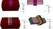
{"title":"Comparative analysis of single and triple material 10 nm Tri-gate FinFET","authors":"Shankhamitra Sunani, Satya Sopan Mahato, Kanjalochan Jena, Raghunandan Swain","doi":"10.1007/s40042-024-01169-6","DOIUrl":null,"url":null,"abstract":"<div><p>A thorough performance analysis of sub-10 nm gate-length Tri-gate Fin-FETs with gates having single material (SMG) and triple material (TMG) has been conducted through technology computer-aided design (TCAD) simulations for low-power applications. The gate of the TMG device is formed of three metals with distinct work functions. To decrease the drain-induced barrier lowering (DIBL) and increase transconductance, the gate work function near the source is higher than near the drain. The DC and analog/RF are obtained, analyzed, and compared between SMG and TMG devices. It is engrossing that, the device’s OFF current (I<sub>OFF</sub>) is drastically reduced and the ON current (I<sub>ON</sub>) is improved in the TMG structure leading to a better switching ratio. Also, TMG Tri-gate FinFET device structures provide an excellent peak transconductance of 5.1756 µA/V at <i>V</i><sub>GS</sub> = 0.16 V and <i>V</i><sub>DS</sub> = 0.1 V, output conductance of 7.45 µA/V at <i>V</i><sub>GS</sub> = 1 V, a subthreshold slope of 120 mV/decade at <i>V</i><sub>DS</sub> = 0.1 V, an I<sub>ON</sub>/I<sub>OFF</sub> ratio of 557.12 at <i>V</i><sub>DS</sub> = 0.1 V, and DIBL of 33 mV/V. Whereas the SMG Tri-gate FinFET has a peak transconductance of 4.28 µA/V at <i>V</i><sub>GS</sub> = 0.4 V and <i>V</i><sub>DS</sub> = 0.1 V, output conductance of 5.88 µA/V at <i>V</i><sub>GS</sub> = 1 V, a subthreshold slope of 300 mV/decade at <i>V</i><sub>DS</sub> = 0.1 V, an I<sub>ON</sub>/I<sub>OFF</sub> ratio of 21.29 at V<sub>DS</sub> = 0.1 V, and DIBL of 55 mV/V.</p></div>","PeriodicalId":677,"journal":{"name":"Journal of the Korean Physical Society","volume":"85 9","pages":"737 - 745"},"PeriodicalIF":0.8000,"publicationDate":"2024-09-04","publicationTypes":"Journal Article","fieldsOfStudy":null,"isOpenAccess":false,"openAccessPdf":"","citationCount":"0","resultStr":null,"platform":"Semanticscholar","paperid":null,"PeriodicalName":"Journal of the Korean Physical Society","FirstCategoryId":"101","ListUrlMain":"https://link.springer.com/article/10.1007/s40042-024-01169-6","RegionNum":4,"RegionCategory":"物理与天体物理","ArticlePicture":[],"TitleCN":null,"AbstractTextCN":null,"PMCID":null,"EPubDate":"","PubModel":"","JCR":"Q3","JCRName":"PHYSICS, MULTIDISCIPLINARY","Score":null,"Total":0}
引用次数: 0
Abstract
A thorough performance analysis of sub-10 nm gate-length Tri-gate Fin-FETs with gates having single material (SMG) and triple material (TMG) has been conducted through technology computer-aided design (TCAD) simulations for low-power applications. The gate of the TMG device is formed of three metals with distinct work functions. To decrease the drain-induced barrier lowering (DIBL) and increase transconductance, the gate work function near the source is higher than near the drain. The DC and analog/RF are obtained, analyzed, and compared between SMG and TMG devices. It is engrossing that, the device’s OFF current (IOFF) is drastically reduced and the ON current (ION) is improved in the TMG structure leading to a better switching ratio. Also, TMG Tri-gate FinFET device structures provide an excellent peak transconductance of 5.1756 µA/V at VGS = 0.16 V and VDS = 0.1 V, output conductance of 7.45 µA/V at VGS = 1 V, a subthreshold slope of 120 mV/decade at VDS = 0.1 V, an ION/IOFF ratio of 557.12 at VDS = 0.1 V, and DIBL of 33 mV/V. Whereas the SMG Tri-gate FinFET has a peak transconductance of 4.28 µA/V at VGS = 0.4 V and VDS = 0.1 V, output conductance of 5.88 µA/V at VGS = 1 V, a subthreshold slope of 300 mV/decade at VDS = 0.1 V, an ION/IOFF ratio of 21.29 at VDS = 0.1 V, and DIBL of 55 mV/V.
期刊介绍:
The Journal of the Korean Physical Society (JKPS) covers all fields of physics spanning from statistical physics and condensed matter physics to particle physics. The manuscript to be published in JKPS is required to hold the originality, significance, and recent completeness. The journal is composed of Full paper, Letters, and Brief sections. In addition, featured articles with outstanding results are selected by the Editorial board and introduced in the online version. For emphasis on aspect of international journal, several world-distinguished researchers join the Editorial board. High quality of papers may be express-published when it is recommended or requested.
 求助内容:
求助内容: 应助结果提醒方式:


