Iterative printing of bulk metal and polymer for additive manufacturing of multi-layer electronic circuits

Zeba Khan, Dheepesh Gururajan, Sabrina Kartmann, Peter Koltay, Roland Zengerle, Zhe Shu
{"title":"Iterative printing of bulk metal and polymer for additive manufacturing of multi-layer electronic circuits","authors":"Zeba Khan, Dheepesh Gururajan, Sabrina Kartmann, Peter Koltay, Roland Zengerle, Zhe Shu","doi":"10.1038/s44334-024-00001-0","DOIUrl":null,"url":null,"abstract":"In pursuing advancing additive manufacturing (AM) techniques for 3D objects, this study combines AM techniques for bulk metal and polymer on a single platform for one-stop printing of multilayer 3D electronic circuits with two novel aspects. The first innovation involves the embedded integration of electronic circuits by printing low-resistance electrical traces from bulk metal into polymer channels. Cross-section grinding results reveal (92 ± 5)% occupancy of electrically conductive traces in polymer channels despite the different thermal properties of the two materials. The second aspect encompasses the possibility of printing vertical bulk metal vias up to 10 mm in height with the potential for expansion, interconnecting electrically conductive traces embedded in different layers of the 3D object. The work provides comprehensive 3D printing design guidelines for successfully integrating fully embedded electrically conductive traces and the interconnecting vertical bulk metal vias. A smooth and continuous workflow is also introduced, enabling a single-run print of functional multilayer embedded 3D electronics. The design rules and the workflow facilitate the iterative printing of two distinct materials, each defined by unique printing temperatures and techniques. Observations indicate that conductive traces using molten metal microdroplets show a 12-fold reduction in resistance compared to nanoparticle ink-based methods, meaning this technique greatly complements multi-material additive manufacturing (MM-AM). The work presents insights into the behavior of molten metal microdroplets on a polymer substrate when printed through the MM-AM process. It explores their characteristics in two scenarios: When they are deposited side-by-side to form conductive traces and when they are deposited out-of-plane to create vertical bulk metal vias. The innovative application of MM-AM to produce multilayer embedded 3D electronics with bulk metal and polymer demonstrates significant potential for realizing the fabrication of free-form 3D electronics.","PeriodicalId":501702,"journal":{"name":"npj Advanced Manufacturing","volume":" ","pages":"1-15"},"PeriodicalIF":0.0000,"publicationDate":"2024-08-28","publicationTypes":"Journal Article","fieldsOfStudy":null,"isOpenAccess":false,"openAccessPdf":"https://www.nature.com/articles/s44334-024-00001-0.pdf","citationCount":"0","resultStr":null,"platform":"Semanticscholar","paperid":null,"PeriodicalName":"npj Advanced Manufacturing","FirstCategoryId":"1085","ListUrlMain":"https://www.nature.com/articles/s44334-024-00001-0","RegionNum":0,"RegionCategory":null,"ArticlePicture":[],"TitleCN":null,"AbstractTextCN":null,"PMCID":null,"EPubDate":"","PubModel":"","JCR":"","JCRName":"","Score":null,"Total":0}
引用次数: 0

Abstract

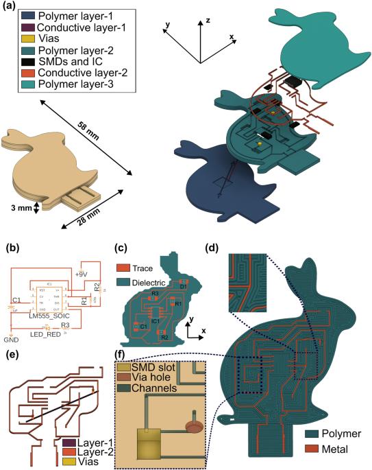
In pursuing advancing additive manufacturing (AM) techniques for 3D objects, this study combines AM techniques for bulk metal and polymer on a single platform for one-stop printing of multilayer 3D electronic circuits with two novel aspects. The first innovation involves the embedded integration of electronic circuits by printing low-resistance electrical traces from bulk metal into polymer channels. Cross-section grinding results reveal (92 ± 5)% occupancy of electrically conductive traces in polymer channels despite the different thermal properties of the two materials. The second aspect encompasses the possibility of printing vertical bulk metal vias up to 10 mm in height with the potential for expansion, interconnecting electrically conductive traces embedded in different layers of the 3D object. The work provides comprehensive 3D printing design guidelines for successfully integrating fully embedded electrically conductive traces and the interconnecting vertical bulk metal vias. A smooth and continuous workflow is also introduced, enabling a single-run print of functional multilayer embedded 3D electronics. The design rules and the workflow facilitate the iterative printing of two distinct materials, each defined by unique printing temperatures and techniques. Observations indicate that conductive traces using molten metal microdroplets show a 12-fold reduction in resistance compared to nanoparticle ink-based methods, meaning this technique greatly complements multi-material additive manufacturing (MM-AM). The work presents insights into the behavior of molten metal microdroplets on a polymer substrate when printed through the MM-AM process. It explores their characteristics in two scenarios: When they are deposited side-by-side to form conductive traces and when they are deposited out-of-plane to create vertical bulk metal vias. The innovative application of MM-AM to produce multilayer embedded 3D electronics with bulk metal and polymer demonstrates significant potential for realizing the fabrication of free-form 3D electronics.
Abstract Image

用于多层电子电路增材制造的块状金属和聚合物迭代打印技术
在追求三维物体增材制造(AM)技术进步的过程中,本研究在单一平台上结合了大块金属和聚合物的 AM 技术,一站式打印多层三维电子电路,并在两个方面进行了创新。第一项创新是通过在聚合物通道中打印大块金属的低电阻电子线路,实现电子电路的嵌入式集成。横截面研磨结果显示,尽管两种材料的热特性不同,但导电迹线在聚合物通道中的占位率为 (92 ± 5)%。第二个方面包括打印高度达 10 毫米的垂直块状金属通孔的可能性,该通孔具有扩展潜力,可将嵌入三维物体不同层中的导电迹线相互连接。这项工作提供了全面的三维打印设计指南,以成功集成完全嵌入式导电迹线和互连垂直块状金属通孔。此外,还介绍了一种平稳、连续的工作流程,可实现功能性多层嵌入式三维电子器件的单次打印。设计规则和工作流程有助于迭代打印两种不同的材料,每种材料都由独特的打印温度和技术定义。观察结果表明,与基于纳米粒子墨水的方法相比,使用熔融金属微滴的导电迹线的电阻降低了 12 倍,这意味着该技术极大地补充了多材料增材制造(MM-AM)的不足。这项研究深入探讨了熔融金属微滴在聚合物基底上通过 MM-AM 工艺打印时的行为。它探讨了两种情况下的特征:当它们并排沉积以形成导电迹线时,以及当它们平面外沉积以形成垂直块状金属通孔时。利用 MM-AM 制作多层嵌体金属和聚合物三维电子器件的创新应用,展示了实现自由形态三维电子器件制造的巨大潜力。
本文章由计算机程序翻译,如有差异,请以英文原文为准。
求助全文
约1分钟内获得全文 求助全文
来源期刊
自引率
0.00%
发文量
0
×
引用
GB/T 7714-2015
复制
MLA
复制
APA
复制
导出至
BibTeX EndNote RefMan NoteFirst NoteExpress
×
提示
您的信息不完整,为了账户安全,请先补充。
现在去补充
×
提示
您因"违规操作"
具体请查看互助需知
我知道了
×
提示
确定
请完成安全验证×
copy
已复制链接
快去分享给好友吧!
我知道了
右上角分享
点击右上角分享
0
联系我们:info@booksci.cn Book学术提供免费学术资源搜索服务,方便国内外学者检索中英文文献。致力于提供最便捷和优质的服务体验。 Copyright © 2023 布克学术 All rights reserved.
京ICP备2023020795号-1
ghs 京公网安备 11010802042870号
Book学术文献互助
Book学术文献互助群
群 号:481959085
Book学术官方微信