Tae-Ho Kim, Dahoon Ahn, Moon G. Lee, Jaehyun Park, Hak-Jun Lee
{"title":"Development of Wafer Bonding System for High Precision Bonding Alignment","authors":"Tae-Ho Kim, Dahoon Ahn, Moon G. Lee, Jaehyun Park, Hak-Jun Lee","doi":"10.1007/s12541-024-01088-3","DOIUrl":null,"url":null,"abstract":"<p>Artificial Intelligence (AI) technology is leading the fourth industrial revolution, particularly as a key element in high-performance computing, complex data analysis, and real-time decision support systems. For the advancement and efficient implementation of these AI technologies, high-performance semiconductor chip manufacturing requires the essential technology of hybrid bonding processes. Hybrid bonding minimizes the physical distance between chips, enabling high-speed data transmission and low power consumption, thereby maximizing AI chip performance. Additionally, this process facilitates chip miniaturization, reduces manufacturing complexity, and supports economical production, thus expanding the application range of AI technologies across various industries. By enabling the integration of multi-functional chips, hybrid bonding significantly improves AI applications in fields such as automotive, healthcare, and telecommunications, contributing to the advancement of the fourth industrial revolution. In this paper, Wafer-to-Wafer (W2W) hybrid bonding system is developed to solve precision degradation issues occurring during the room-temperature hybrid bonding process. Performance evaluation and experiments conducted on the bonding system, fabricated based on optimal design, confirmed high-precision bonding performance at room temperature through precise position control to be compensate position error of wafer bonding.</p>","PeriodicalId":14359,"journal":{"name":"International Journal of Precision Engineering and Manufacturing","volume":"46 1","pages":""},"PeriodicalIF":3.6000,"publicationDate":"2024-08-06","publicationTypes":"Journal Article","fieldsOfStudy":null,"isOpenAccess":false,"openAccessPdf":"","citationCount":"0","resultStr":null,"platform":"Semanticscholar","paperid":null,"PeriodicalName":"International Journal of Precision Engineering and Manufacturing","FirstCategoryId":"5","ListUrlMain":"https://doi.org/10.1007/s12541-024-01088-3","RegionNum":4,"RegionCategory":"工程技术","ArticlePicture":[],"TitleCN":null,"AbstractTextCN":null,"PMCID":null,"EPubDate":"","PubModel":"","JCR":"Q2","JCRName":"Engineering","Score":null,"Total":0}
引用次数: 0
Abstract
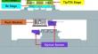
Artificial Intelligence (AI) technology is leading the fourth industrial revolution, particularly as a key element in high-performance computing, complex data analysis, and real-time decision support systems. For the advancement and efficient implementation of these AI technologies, high-performance semiconductor chip manufacturing requires the essential technology of hybrid bonding processes. Hybrid bonding minimizes the physical distance between chips, enabling high-speed data transmission and low power consumption, thereby maximizing AI chip performance. Additionally, this process facilitates chip miniaturization, reduces manufacturing complexity, and supports economical production, thus expanding the application range of AI technologies across various industries. By enabling the integration of multi-functional chips, hybrid bonding significantly improves AI applications in fields such as automotive, healthcare, and telecommunications, contributing to the advancement of the fourth industrial revolution. In this paper, Wafer-to-Wafer (W2W) hybrid bonding system is developed to solve precision degradation issues occurring during the room-temperature hybrid bonding process. Performance evaluation and experiments conducted on the bonding system, fabricated based on optimal design, confirmed high-precision bonding performance at room temperature through precise position control to be compensate position error of wafer bonding.
期刊介绍:
The International Journal of Precision Engineering and Manufacturing accepts original contributions on all aspects of precision engineering and manufacturing. The journal specific focus areas include, but are not limited to:
- Precision Machining Processes
- Manufacturing Systems
- Robotics and Automation
- Machine Tools
- Design and Materials
- Biomechanical Engineering
- Nano/Micro Technology
- Rapid Prototyping and Manufacturing
- Measurements and Control
Surveys and reviews will also be planned in consultation with the Editorial Board.
 求助内容:
求助内容: 应助结果提醒方式:


