Tuning the electronic structure of monolayer MoS2 towards metal like via vanadium doping

IF 3.1 3区 材料科学 Q2 MATERIALS SCIENCE, MULTIDISCIPLINARY
Dipak Maity, Rahul Sharma, Krishna Rani Sahoo, Ashique Lal, Raul Arenal, Tharangattu N. Narayanan
{"title":"Tuning the electronic structure of monolayer MoS2 towards metal like via vanadium doping","authors":"Dipak Maity, Rahul Sharma, Krishna Rani Sahoo, Ashique Lal, Raul Arenal, Tharangattu N. Narayanan","doi":"10.1103/physrevmaterials.8.084002","DOIUrl":null,"url":null,"abstract":"Doping of two-dimensional layered semiconducting materials is becoming pivotal in tailoring their electronic properties, enabling the development of advanced electronic and optoelectronic devices, where the selection of dopant is important. Here, we demonstrate the potential of substitutional vanadium (V) doping in monolayer molybdenum disulfide (<math xmlns=\"http://www.w3.org/1998/Math/MathML\"><mrow><mi>Mo</mi><msub><mi mathvariant=\"normal\">S</mi><mn>2</mn></msub></mrow></math>) lattice in different extents leading to tunable electronic and optoelectronic properties. We found that low-level V doping (∼1 <math xmlns=\"http://www.w3.org/1998/Math/MathML\"><mrow><mtext>at.</mtext><mspace width=\"0.16em\"></mspace><mo>%</mo></mrow></math>) induces <math xmlns=\"http://www.w3.org/1998/Math/MathML\"><mi>p</mi></math>-type characteristics in otherwise <math xmlns=\"http://www.w3.org/1998/Math/MathML\"><mi>n</mi></math>-type monolayer <math xmlns=\"http://www.w3.org/1998/Math/MathML\"><mrow><mi>Mo</mi><msub><mi mathvariant=\"normal\">S</mi><mn>2</mn></msub></mrow></math>, whereas medium-level doping (∼5 <math xmlns=\"http://www.w3.org/1998/Math/MathML\"><mrow><mtext>at.</mtext><mspace width=\"0.16em\"></mspace><mo>%</mo></mrow></math>) leads to an ambipolar semiconductor. Degenerately doped <math xmlns=\"http://www.w3.org/1998/Math/MathML\"><mrow><mi>Mo</mi><msub><mi mathvariant=\"normal\">S</mi><mn>2</mn></msub></mrow></math> (∼9 <math xmlns=\"http://www.w3.org/1998/Math/MathML\"><mrow><mtext>at.</mtext><mspace width=\"0.16em\"></mspace><mo>%</mo></mrow></math>) facilitates a transition from semiconducting towards metallic (metal-like) with reduced electrical resistivity (∼4.5 <math xmlns=\"http://www.w3.org/1998/Math/MathML\"><mrow><mi mathvariant=\"normal\">Ω</mi><mspace width=\"0.16em\"></mspace><mtext>m</mtext></mrow></math> of <math xmlns=\"http://www.w3.org/1998/Math/MathML\"><mrow><mi>Mo</mi><msub><mi mathvariant=\"normal\">S</mi><mn>2</mn></msub></mrow></math> to <math xmlns=\"http://www.w3.org/1998/Math/MathML\"><mrow><mo>∼</mo><mn>2.2</mn><mo>×</mo><msup><mrow><mn>10</mn></mrow><mrow><mo>−</mo><mn>5</mn></mrow></msup><mi mathvariant=\"normal\">Ω</mi><mspace width=\"0.16em\"></mspace><mtext>m</mtext></mrow></math>), low activation energy for transport (∼11 meV), and electric field independent drain current in field effect transistor–based transfer characteristics. A detailed temperature- and power-dependent photoluminescence study along with density functional theory–based calculations in support unravels the emergence of an excitonic transition at ∼850 nm with its intensity dependent on the amount of vanadium. This study shows the potential of V doping in <math xmlns=\"http://www.w3.org/1998/Math/MathML\"><mrow><mi>Mo</mi><msub><mi mathvariant=\"normal\">S</mi><mn>2</mn></msub></mrow></math> for generating multifunctional two-dimensional materials for next generation electronics, optoelectronics, and interconnects with systematic control over its electronic structure in a wide range.","PeriodicalId":20545,"journal":{"name":"Physical Review Materials","volume":null,"pages":null},"PeriodicalIF":3.1000,"publicationDate":"2024-08-07","publicationTypes":"Journal Article","fieldsOfStudy":null,"isOpenAccess":false,"openAccessPdf":"","citationCount":"0","resultStr":null,"platform":"Semanticscholar","paperid":null,"PeriodicalName":"Physical Review Materials","FirstCategoryId":"88","ListUrlMain":"https://doi.org/10.1103/physrevmaterials.8.084002","RegionNum":3,"RegionCategory":"材料科学","ArticlePicture":[],"TitleCN":null,"AbstractTextCN":null,"PMCID":null,"EPubDate":"","PubModel":"","JCR":"Q2","JCRName":"MATERIALS SCIENCE, MULTIDISCIPLINARY","Score":null,"Total":0}
引用次数: 0

Abstract

Doping of two-dimensional layered semiconducting materials is becoming pivotal in tailoring their electronic properties, enabling the development of advanced electronic and optoelectronic devices, where the selection of dopant is important. Here, we demonstrate the potential of substitutional vanadium (V) doping in monolayer molybdenum disulfide (MoS2) lattice in different extents leading to tunable electronic and optoelectronic properties. We found that low-level V doping (∼1 at.%) induces p-type characteristics in otherwise n-type monolayer MoS2, whereas medium-level doping (∼5 at.%) leads to an ambipolar semiconductor. Degenerately doped MoS2 (∼9 at.%) facilitates a transition from semiconducting towards metallic (metal-like) with reduced electrical resistivity (∼4.5 Ωm of MoS2 to 2.2×10⁵Ωm), low activation energy for transport (∼11 meV), and electric field independent drain current in field effect transistor–based transfer characteristics. A detailed temperature- and power-dependent photoluminescence study along with density functional theory–based calculations in support unravels the emergence of an excitonic transition at ∼850 nm with its intensity dependent on the amount of vanadium. This study shows the potential of V doping in MoS2 for generating multifunctional two-dimensional materials for next generation electronics, optoelectronics, and interconnects with systematic control over its electronic structure in a wide range.
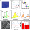
Abstract Image

通过掺杂钒调谐单层 MoS2 的电子结构,使其趋向于类金属结构
二维层状半导体材料的掺杂正在成为调整其电子特性的关键,从而使先进电子和光电设备的开发成为可能,而掺杂剂的选择在其中起着重要作用。在这里,我们展示了在单层二硫化钼(MoS2)晶格中不同程度地掺入替代钒(V)的潜力,从而获得可调的电子和光电特性。我们发现,低浓度掺钒(1%∼1%)会在原本为 n 型的单层 MoS2 中诱导出 p 型特性,而中浓度掺钒(5%∼5%)则会导致产生双极性半导体。去极掺杂的 MoS2(∼9 at.%)促进了从半导体向金属(类金属)的过渡,电阻率降低(MoS2 的电阻率从 4.5 Ωm 降低到 2.2×10⁻⁵Ωm),传输活化能降低(∼11 meV),在基于场效应晶体管的传输特性中,漏极电流与电场无关。详细的温度和功率依赖性光致发光研究以及基于密度泛函理论的计算揭示了在∼850 nm处出现的激子跃迁,其强度取决于钒的含量。这项研究显示了在 MoS2 中掺入钒的潜力,通过对其电子结构进行大范围的系统控制,可为下一代电子、光电和互连器件生成多功能二维材料。
本文章由计算机程序翻译,如有差异,请以英文原文为准。
求助全文
约1分钟内获得全文 求助全文
来源期刊
Physical Review Materials
Physical Review Materials Physics and Astronomy-Physics and Astronomy (miscellaneous)
CiteScore
5.80
自引率
5.90%
发文量
611
期刊介绍: Physical Review Materials is a new broad-scope international journal for the multidisciplinary community engaged in research on materials. It is intended to fill a gap in the family of existing Physical Review journals that publish materials research. This field has grown rapidly in recent years and is increasingly being carried out in a way that transcends conventional subject boundaries. The journal was created to provide a common publication and reference source to the expanding community of physicists, materials scientists, chemists, engineers, and researchers in related disciplines that carry out high-quality original research in materials. It will share the same commitment to the high quality expected of all APS publications.
×
引用
GB/T 7714-2015
复制
MLA
复制
APA
复制
导出至
BibTeX EndNote RefMan NoteFirst NoteExpress
×
提示
您的信息不完整,为了账户安全,请先补充。
现在去补充
×
提示
您因"违规操作"
具体请查看互助需知
我知道了
×
提示
确定
请完成安全验证×
copy
已复制链接
快去分享给好友吧!
我知道了
右上角分享
点击右上角分享
0
联系我们:info@booksci.cn Book学术提供免费学术资源搜索服务,方便国内外学者检索中英文文献。致力于提供最便捷和优质的服务体验。 Copyright © 2023 布克学术 All rights reserved.
京ICP备2023020795号-1
ghs 京公网安备 11010802042870号
Book学术文献互助
Book学术文献互助群
群 号:481959085
Book学术官方微信