Fabrication of Multi-Material Functional Circuits Using Microfluidic Directed Materials Patterning
引用次数: 0
Abstract
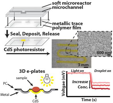
Traditional circuit board fabrication schemes are not directly applicable to the production of flexible, multi-material circuits. This article reports a technique, microfluidic directed material patterning, which combines soft microfluidic stamps and low-temperature solution-phase deposition to generate multi-material circuits on flexible, non-planar polymeric supports. Specifically, metallic and semiconductive traces are combined on commodity plastic films to yield functional photosensitive circuits that can be used in the spectrophotometric detection and concentration measurement of microdroplets on 3D “e-plates.” The photoresistive material cadmium sulfide is used in these circuits because it is suitable for visible light detection and it can be deposited directly from aqueous solutions following established bath deposition procedures. This method can produce colorimetric devices capable of quantifying micromolar concentrations of Allura Red in microdroplets of Kool-Aid. This technique presents the opportunity for producing single-use or low-use disposable/recyclable devices for flexible 3D sensors and detectors following a convenient, low-waste fabrication scheme. The general capabilities of this approach, in terms of substrate geometry and device layout (e.g., the number, area, and pattern of photoresistive elements), can be applied to the design and manufacture of more intricate, multiplexed devices supportive of advanced and/or specialized functions that go beyond those reported in this initial demonstration.
利用微流体定向材料图案化制造多材料功能电路
传统的电路板制造方案无法直接用于柔性多材料电路的生产。本文报道了一种微流体定向材料图案化技术,该技术结合了软性微流体印章和低温溶液相沉积技术,可在柔性非平面聚合物支架上生成多材料电路。具体来说,在商品塑料薄膜上结合金属和半导体迹线,生成功能性光敏电路,可用于三维 "电子板 "上微滴的分光光度检测和浓度测量。这些电路中使用了光敏材料硫化镉,因为它适用于可见光检测,而且可以按照既定的浴沉积程序直接从水溶液中沉积出来。这种方法可以生产出比色装置,能够量化酷爱饮料微滴中的微摩尔浓度 Allura Red。这项技术提供了一个机会,可以按照便捷、低废物的制造方案,为灵活的三维传感器和探测器生产一次性或低用量的一次性/可回收装置。这种方法在基底几何和器件布局(如光阻元件的数量、面积和模式)方面的一般能力,可用于设计和制造更复杂、支持高级和/或特殊功能的多路复用器件,其功能超出了本次初步演示所报告的范围。
本文章由计算机程序翻译,如有差异,请以英文原文为准。
求助全文
约1分钟内获得全文
求助全文

 求助内容:
求助内容: 应助结果提醒方式:


