Atomic-level precision creation and manipulation of interfacial Se chemisorbates in graphene/WSe2 heterostructures
IF 3.7
2区 物理与天体物理
Q1 Physics and Astronomy
引用次数: 0
Abstract
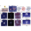
It has long been an ultimate goal to introduce chemical doping at the atomic level to precisely tune properties of materials. Two-dimensional materials have a natural advantage due to their high surface to volume ratio, but achieving this goal experimentally remains a huge challenge. Here, we demonstrate the ability to introduce chemical doping in graphene with atomic-level precision by controlling chemical adsorption of individual Se atoms, which are extracted from the that is underneath, at the interface of the heterostructures. Our scanning tunneling microscopy (STM) measurements, combined with first-principles calculations, reveal that individual Se atoms can chemisorb on three possible positions in graphene, which generate distinct pseudospin-mediated atomic-scale vortices in graphene. Furthermore, the chemisorbed positions of individual Se atoms can be manipulated by the STM tip, which enables us to achieve atomic-scale control of quantum interference of the pseudospin-mediated vortices in graphene. This result offers the promise of controlling properties of materials with atomic-level precision through chemical doping.
在石墨烯/WSe2 异质结构中原子级精确创建和操纵界面硒化学吸附剂
长期以来,在原子层面引入化学掺杂以精确调节材料特性一直是我们的终极目标。二维材料具有高表面体积比的天然优势,但要在实验中实现这一目标仍是一个巨大的挑战。在这里,我们展示了通过控制石墨烯/WSe2 异质结构界面上单个 Se 原子的化学吸附,在石墨烯中引入原子级精度的化学掺杂的能力。我们的扫描隧道显微镜(STM)测量结果与第一原理计算相结合,揭示了单个硒原子可以在石墨烯的三个可能位置上发生化学吸附,从而在石墨烯中产生不同的伪ospin 介导的原子尺度漩涡。此外,单个硒原子的化学吸附位置可以通过 STM 针尖进行操纵,这使我们能够实现对石墨烯中伪斯宾介导的漩涡的原子尺度量子干涉控制。这一结果为通过化学掺杂以原子级精度控制材料特性带来了希望。
本文章由计算机程序翻译,如有差异,请以英文原文为准。
求助全文
约1分钟内获得全文
求助全文
来源期刊
Physical Review B
物理-物理:凝聚态物理
CiteScore
6.70
自引率
32.40%
发文量
0
审稿时长
3.0 months
期刊介绍:
Physical Review B (PRB) is the world’s largest dedicated physics journal, publishing approximately 100 new, high-quality papers each week. The most highly cited journal in condensed matter physics, PRB provides outstanding depth and breadth of coverage, combined with unrivaled context and background for ongoing research by scientists worldwide.
PRB covers the full range of condensed matter, materials physics, and related subfields, including:
-Structure and phase transitions
-Ferroelectrics and multiferroics
-Disordered systems and alloys
-Magnetism
-Superconductivity
-Electronic structure, photonics, and metamaterials
-Semiconductors and mesoscopic systems
-Surfaces, nanoscience, and two-dimensional materials
-Topological states of matter
文献相关原料
| 公司名称 | 产品信息 | 采购帮参考价格 |
|---|
 求助内容:
求助内容: 应助结果提醒方式:


