Inorganic Cs3Bi2I9 lead-free halide perovskite film for large-area X-ray detector via low-cost ambient spray coating
IF 8.3
2区 材料科学
Q1 MATERIALS SCIENCE, MULTIDISCIPLINARY
引用次数: 0
Abstract
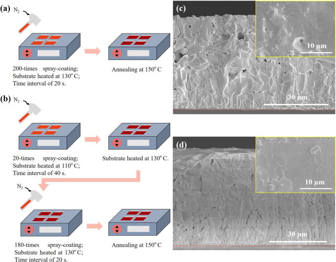
Lead-free Cs3Bi2I9 single crystals have been demonstrated to be promising materials for direct X-ray detectors with remarkable performance. However, their application for 2D X-ray imaging is hindered by their time-consuming preparation and limited crystal size. In this paper, a thick Cs3Bi2I9 perovskite film fabricated via facile spray coating at a low processing temperature, which increases the area of the photoactive film, reduces the processing time, decreases the energy budget and the production cost, and enhances the production yield due to high material utilization, has great potential for commercial applications. Careful control of the processing temperature and intervals during spray coating results in a dense and thick perovskite film with well-stacked perovskite domains. The compact perovskite film enhances the charge transport capability of the Cs3Bi2I9 perovskite film and reduces the dark current density of the X-ray detector. The resultant X-ray detector, prepared through a two-step spray coating process, exhibited a sensitivity of 127.23 μC Gyair−1 cm−2 and a detection limit of 7.4 μGyair s−1. In addition, the device delivers long-term stability with a consistent photoresponse when exposed to consecutive X-ray pulse irradiation. A two-step spray coating process (first step: 20 cycles of spray coating at 110 °C with 40 s intervals; second step: 180 cycles of spray coating at 130 °C with 20 s intervals) was employed to a produce large-area, compact, and thick Cs3Bi2I9 perovskite film for the application of direct X-ray detectors. The fabricated device achieved a large active area of 150 mm2, a sensitivity of 127.23 μC Gyair−1 cm−2, a detection limit of 7.4 μGyairs−1, and durability after long-term X-ray pulse irradiation.


用于大面积 X 射线探测器的无机 Cs3Bi2I9 无铅卤化物包晶薄膜(通过低成本环境喷雾涂层实现
无铅 Cs3Bi2I9 单晶已被证明是性能卓越的直接 X 射线探测器的理想材料。然而,它们在二维 X 射线成像中的应用却因制备耗时和晶体尺寸有限而受到阻碍。本文在低加工温度下通过简便的喷涂方法制备了厚的 Cs3Bi2I9 包晶石薄膜,增加了光活性薄膜的面积,缩短了加工时间,降低了能源预算和生产成本,并因材料利用率高而提高了产量,具有巨大的商业应用潜力。在喷涂过程中,对加工温度和间隔时间的精心控制可获得致密厚实、包晶畴堆积良好的包晶薄膜。致密的包晶薄膜增强了 Cs3Bi2I9 包晶薄膜的电荷传输能力,降低了 X 射线探测器的暗电流密度。通过两步喷涂工艺制备的 X 射线探测器的灵敏度为 127.23 μC Gyair-1 cm-2,探测极限为 7.4 μGyair s-1。此外,该装置在连续接受 X 射线脉冲照射时具有长期稳定性和一致的光响应。
本文章由计算机程序翻译,如有差异,请以英文原文为准。
求助全文
约1分钟内获得全文
求助全文
来源期刊

Npg Asia Materials
MATERIALS SCIENCE, MULTIDISCIPLINARY-
CiteScore
15.40
自引率
1.00%
发文量
87
审稿时长
2 months
期刊介绍:
NPG Asia Materials is an open access, international journal that publishes peer-reviewed review and primary research articles in the field of materials sciences. The journal has a global outlook and reach, with a base in the Asia-Pacific region to reflect the significant and growing output of materials research from this area. The target audience for NPG Asia Materials is scientists and researchers involved in materials research, covering a wide range of disciplines including physical and chemical sciences, biotechnology, and nanotechnology. The journal particularly welcomes high-quality articles from rapidly advancing areas that bridge the gap between materials science and engineering, as well as the classical disciplines of physics, chemistry, and biology. NPG Asia Materials is abstracted/indexed in Journal Citation Reports/Science Edition Web of Knowledge, Google Scholar, Chemical Abstract Services, Scopus, Ulrichsweb (ProQuest), and Scirus.
 求助内容:
求助内容: 应助结果提醒方式:


