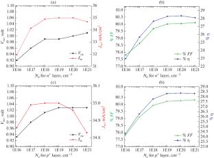
{"title":"An Insight Analysis of In0.7Ga0.3N Based pn Homo-Junction Solar Cell using SCAPS-1D Simulation Software","authors":"Arman Rahman, Emran Hossain, Sakhawat Hussain","doi":"10.3103/S0003701X23600522","DOIUrl":null,"url":null,"abstract":"<p>An insight analysis of In<sub>0.7</sub>Ga<sub>0.3</sub>N based pn homo-junction solar cell structure has been carried out using simulation software. A novel solar cell structure of <i>n</i>+ buffer contact layer/<i>n</i> window layer/<i>p</i> absorber layer/<i>p</i>+ back absorber layer has been proposed after device optimization. We have found that under the sun spectrum of AM 1.5 of 1 KW/m<sup>2</sup> operating at 300 K, the solar cell with low series resistance of 3 Ω cm<sup>2</sup>, highly doped (1×10<sup>19</sup> cm<sup>–3</sup>) <i>n</i>+ layer as buffer contact layer and <i>p</i>+ layer of 200 nm thick as back absorber layer on top of back metal contact, enable us to achieve an efficient solar cell. We found that doping concentration of <span>\\(1 \\times {{10}^{{16}}}{\\text{ c}}{{{\\text{m}}}^{{ - 3}}}\\)</span> in both active n and p layer, with 30 nm and 1.0 <span>\\({{\\mu m}}\\)</span> of thickness, respectively, would allow us to achieve short circuit current density of <span>\\(35{{{\\text{ mA}}} \\mathord{\\left/ {\\vphantom {{{\\text{mA}}} {{\\text{c}}{{{\\text{m}}}^{2}}}}} \\right. \\kern-0em} {{\\text{c}}{{{\\text{m}}}^{2}}}}\\)</span>, open circuit voltage of 1.0 V, overall efficiency of 28.32% and fill factor value of 80% from the solar cell. If we could further reduce the series resistance of In<sub>0.7</sub>Ga<sub>0.3</sub>N pn homo-junction solar cell to ideal one, it may allow us to have even higher overall efficiency and fill factor values of 31 and 86%, respectively.</p>","PeriodicalId":475,"journal":{"name":"Applied Solar Energy","volume":"59 6","pages":"818 - 827"},"PeriodicalIF":1.2040,"publicationDate":"2024-03-23","publicationTypes":"Journal Article","fieldsOfStudy":null,"isOpenAccess":false,"openAccessPdf":"","citationCount":"0","resultStr":null,"platform":"Semanticscholar","paperid":null,"PeriodicalName":"Applied Solar Energy","FirstCategoryId":"1","ListUrlMain":"https://link.springer.com/article/10.3103/S0003701X23600522","RegionNum":0,"RegionCategory":null,"ArticlePicture":[],"TitleCN":null,"AbstractTextCN":null,"PMCID":null,"EPubDate":"","PubModel":"","JCR":"Q3","JCRName":"Energy","Score":null,"Total":0}
引用次数: 0
Abstract
An insight analysis of In0.7Ga0.3N based pn homo-junction solar cell structure has been carried out using simulation software. A novel solar cell structure of n+ buffer contact layer/n window layer/p absorber layer/p+ back absorber layer has been proposed after device optimization. We have found that under the sun spectrum of AM 1.5 of 1 KW/m2 operating at 300 K, the solar cell with low series resistance of 3 Ω cm2, highly doped (1×1019 cm–3) n+ layer as buffer contact layer and p+ layer of 200 nm thick as back absorber layer on top of back metal contact, enable us to achieve an efficient solar cell. We found that doping concentration of \(1 \times {{10}^{{16}}}{\text{ c}}{{{\text{m}}}^{{ - 3}}}\) in both active n and p layer, with 30 nm and 1.0 \({{\mu m}}\) of thickness, respectively, would allow us to achieve short circuit current density of \(35{{{\text{ mA}}} \mathord{\left/ {\vphantom {{{\text{mA}}} {{\text{c}}{{{\text{m}}}^{2}}}}} \right. \kern-0em} {{\text{c}}{{{\text{m}}}^{2}}}}\), open circuit voltage of 1.0 V, overall efficiency of 28.32% and fill factor value of 80% from the solar cell. If we could further reduce the series resistance of In0.7Ga0.3N pn homo-junction solar cell to ideal one, it may allow us to have even higher overall efficiency and fill factor values of 31 and 86%, respectively.
期刊介绍:
Applied Solar Energy is an international peer reviewed journal covers various topics of research and development studies on solar energy conversion and use: photovoltaics, thermophotovoltaics, water heaters, passive solar heating systems, drying of agricultural production, water desalination, solar radiation condensers, operation of Big Solar Oven, combined use of solar energy and traditional energy sources, new semiconductors for solar cells and thermophotovoltaic system photocells, engines for autonomous solar stations.
 求助内容:
求助内容: 应助结果提醒方式:


