Gate-Tunable Short-Wave Infrared Polycrystalline GeSn Phototransistors on Noncrystalline Substrates
IF 8.3
2区 材料科学
Q1 MATERIALS SCIENCE, MULTIDISCIPLINARY
引用次数: 0
Abstract
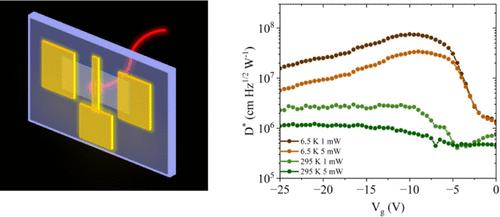
GeSn is a group-IV alloy with immense potential to advance microelectronics technology due to its intrinsic compatibility with existing Si CMOS processes. With a sufficiently high Sn composition, GeSn is classified as a direct bandgap semiconductor. Polycrystalline GeSn holds several additional advantages, including its significantly lower synthesis cost compared to its epitaxial counterpart, as well as the versatility to grow these films on a variety of substrates. Here, we present a polycrystalline thin-film GeSn phototransistor on a fused silica substrate with a Sn composition of ∼10%, showing a photoresponse in the short-wave infrared wavelength range, critical for emerging sensing applications. This device shows a gate-tunable response, with responsivities approaching up to 1.7 mA/W with only a 30 nm-thick GeSn layer. Furthermore, phototransistors offer additional adaptability through gating, which allows for the reduction of dark current. This not only enhances the signal-to-noise ratio but also offers more flexible integration with various image sensor readout implementations using different substrates. The specific detectivity of this phototransistor is within an order of magnitude of those of previously reported GeSn photodetectors grown by molecular beam epitaxy and chemical vapor deposition, even though the absorber is 3 to 20× thinner while the electrode spacing for photocarrier transport is approximately 15× longer than the carrier diffusion length in this work, showing great potential benefits of extending similar device structures to epitaxial GeSn layers. As these GeSn phototransistors utilize a noncrystalline substrate, our work establishes a fundamentally more versatile path toward monolithically integrated GeSn-based photodetectors for next-generation multimodal sensors.
求助全文
约1分钟内获得全文
求助全文
来源期刊

ACS Applied Materials & Interfaces
工程技术-材料科学:综合
CiteScore
16.00
自引率
6.30%
发文量
4978
审稿时长
1.8 months
期刊介绍:
ACS Applied Materials & Interfaces is a leading interdisciplinary journal that brings together chemists, engineers, physicists, and biologists to explore the development and utilization of newly-discovered materials and interfacial processes for specific applications. Our journal has experienced remarkable growth since its establishment in 2009, both in terms of the number of articles published and the impact of the research showcased. We are proud to foster a truly global community, with the majority of published articles originating from outside the United States, reflecting the rapid growth of applied research worldwide.
 求助内容:
求助内容: 应助结果提醒方式:


