Size Effect of Negative Capacitance State and Subthreshold Swing in Van der Waals Ferrielectric Field-Effect Transistors

IF 5.3 2区 材料科学 Q2 MATERIALS SCIENCE, MULTIDISCIPLINARY
Anna N. Morozovska, Eugene A. Eliseev, Yulian M. Vysochanskii, Sergei V. Kalinin, Maksym V. Strikha
{"title":"Size Effect of Negative Capacitance State and Subthreshold Swing in Van der Waals Ferrielectric Field-Effect Transistors","authors":"Anna N. Morozovska, Eugene A. Eliseev, Yulian M. Vysochanskii, Sergei V. Kalinin, Maksym V. Strikha","doi":"10.1002/aelm.202400495","DOIUrl":null,"url":null,"abstract":"Analytical calculations corroborated by the finite element modeling show that thin films of Van der Waals ferrielectrics covered by a 2D-semiconductor are promising candidates for the controllable reduction of the dielectric layer capacitance due to the negative capacitance (NC) effect emerging in the thin films. The NC state is conditioned by energy-degenerated poly-domain states of the ferrielectric polarization induced in the films under incomplete screening conditions in the presence of a dielectric layer. Calculations performed for the FET-type heterostructure “ferrielectric CuInP<sub>2</sub>S<sub>6</sub> film—2D-MoS<sub>2</sub> single-layer—SiO<sub>2</sub> dielectric layer” reveal the pronounced size effect of the multilayer capacitance. Derived analytical expressions for the electric polarization and multilayer capacitance allow to predict the thickness range of the dielectric layer and ferrielectric film for which the NC effect is the most pronounced in various Van der Waals ferrielectrics, and the corresponding subthreshold swing becomes much less than the Boltzmann's limit. Obtained results can be useful for the size and temperature control of the NC effect in the steep-slope ferrielectric FETs.","PeriodicalId":110,"journal":{"name":"Advanced Electronic Materials","volume":"66 1","pages":""},"PeriodicalIF":5.3000,"publicationDate":"2024-10-22","publicationTypes":"Journal Article","fieldsOfStudy":null,"isOpenAccess":false,"openAccessPdf":"","citationCount":"0","resultStr":null,"platform":"Semanticscholar","paperid":null,"PeriodicalName":"Advanced Electronic Materials","FirstCategoryId":"88","ListUrlMain":"https://doi.org/10.1002/aelm.202400495","RegionNum":2,"RegionCategory":"材料科学","ArticlePicture":[],"TitleCN":null,"AbstractTextCN":null,"PMCID":null,"EPubDate":"","PubModel":"","JCR":"Q2","JCRName":"MATERIALS SCIENCE, MULTIDISCIPLINARY","Score":null,"Total":0}
引用次数: 0

Abstract

Analytical calculations corroborated by the finite element modeling show that thin films of Van der Waals ferrielectrics covered by a 2D-semiconductor are promising candidates for the controllable reduction of the dielectric layer capacitance due to the negative capacitance (NC) effect emerging in the thin films. The NC state is conditioned by energy-degenerated poly-domain states of the ferrielectric polarization induced in the films under incomplete screening conditions in the presence of a dielectric layer. Calculations performed for the FET-type heterostructure “ferrielectric CuInP2S6 film—2D-MoS2 single-layer—SiO2 dielectric layer” reveal the pronounced size effect of the multilayer capacitance. Derived analytical expressions for the electric polarization and multilayer capacitance allow to predict the thickness range of the dielectric layer and ferrielectric film for which the NC effect is the most pronounced in various Van der Waals ferrielectrics, and the corresponding subthreshold swing becomes much less than the Boltzmann's limit. Obtained results can be useful for the size and temperature control of the NC effect in the steep-slope ferrielectric FETs.
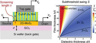
Abstract Image

范德瓦尔斯铁电场效应晶体管的负电容状态和阈下波动的尺寸效应
有限元建模证实的分析计算表明,由于薄膜中出现的负电容(NC)效应,被二维半导体覆盖的范德瓦尔斯铁电薄膜是可控降低介电层电容的理想候选材料。负电容状态由薄膜在介电层存在的不完全屏蔽条件下诱发的铁电极化的能量消耗多域状态决定。对 FET 型异质结构 "铁电 CuInP2S6 薄膜-2D-MoS2 单层-二氧化硅介电层 "进行的计算表明,多层电容的尺寸效应非常明显。推导出的电极化和多层电容分析表达式可以预测介电层和铁电薄膜的厚度范围,在各种范德华铁电中,NC 效应最为明显,相应的次阈值摆幅也远小于玻尔兹曼极限。所获得的结果有助于控制陡坡铁电场效应晶体管中 NC 效应的大小和温度。
本文章由计算机程序翻译,如有差异,请以英文原文为准。
求助全文
约1分钟内获得全文 求助全文
来源期刊
Advanced Electronic Materials
Advanced Electronic Materials NANOSCIENCE & NANOTECHNOLOGYMATERIALS SCIE-MATERIALS SCIENCE, MULTIDISCIPLINARY
CiteScore
11.00
自引率
3.20%
发文量
433
期刊介绍: Advanced Electronic Materials is an interdisciplinary forum for peer-reviewed, high-quality, high-impact research in the fields of materials science, physics, and engineering of electronic and magnetic materials. It includes research on physics and physical properties of electronic and magnetic materials, spintronics, electronics, device physics and engineering, micro- and nano-electromechanical systems, and organic electronics, in addition to fundamental research.
×
引用
GB/T 7714-2015
复制
MLA
复制
APA
复制
导出至
BibTeX EndNote RefMan NoteFirst NoteExpress
×
提示
您的信息不完整,为了账户安全,请先补充。
现在去补充
×
提示
您因"违规操作"
具体请查看互助需知
我知道了
×
提示
确定
请完成安全验证×
copy
已复制链接
快去分享给好友吧!
我知道了
右上角分享
点击右上角分享
0
联系我们:info@booksci.cn Book学术提供免费学术资源搜索服务,方便国内外学者检索中英文文献。致力于提供最便捷和优质的服务体验。 Copyright © 2023 布克学术 All rights reserved.
京ICP备2023020795号-1
ghs 京公网安备 11010802042870号
Book学术文献互助
Book学术文献互助群
群 号:481959085
Book学术官方微信