Submicron Embedded Air/GaN Diffraction Gratings for Photonic Applications
IF 5.3
2区 材料科学
Q2 MATERIALS SCIENCE, MULTIDISCIPLINARY
引用次数: 0
Abstract
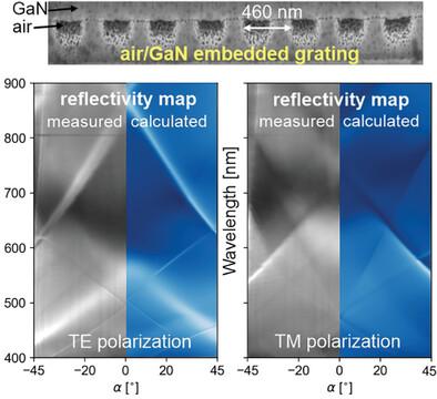
The integration of photonic elements with nitride optoelectronic structures allows control of emitted light properties, which is advantageous for achieving, e.g., a single wavelength lasing. Positioning of the photonic structures on the top surface of GaN-based devices is problematic, in particular, for deposition of a metal contact to p-type top layer. In this work, custom-shaped submicron air channels arranged periodically 150 nm below the sample surface, forming an air/GaN diffraction grating embedded within a volume of the structure is proposed and fabricated. The fabrication process includes selective area Si ion implantation, GaN regrowth using plasma-assisted molecular beam epitaxy, ultra-high-pressure annealing for efficient electrical activation of implanted Si without diffusion, and electrochemical etching for the removal of selectively doped material. Embedded air/GaN diffraction gratings with periodicity of 460 and 631 nm are shown. Width of air channels ranges from 46 to 320 nm. Angle and polarization resolved reflectivity measurements combined with theoretical modeling confirm the designed optical performance of the embedded diffraction gratings in the GaN volume. The presented design and fabrication of custom-shaped, fully integrated photonic structures buried below the surface paves the way for novel type constructions of optoelectronic devices, such as compact distributed feedback laser diodes

用于光子应用的亚微米级嵌入式空气/氮化镓衍射光栅
将光子元件与氮化物光电结构整合在一起,可以控制发射光的特性,这对于实现单波长激光等非常有利。光子结构在氮化镓基器件顶面的定位存在问题,特别是在 p 型顶层沉积金属触点时。在这项工作中,我们提出并制作了定制形状的亚微米空气通道,在样品表面下 150 nm 处周期性排列,形成一个空气/氮化镓衍射光栅,嵌入结构的一个体积内。制造过程包括选择性区域硅离子注入、利用等离子体辅助分子束外延技术实现氮化镓再生长、超高压退火以实现植入硅的高效电活化而不发生扩散,以及电化学蚀刻以去除选择性掺杂的材料。图中显示了周期为 460 纳米和 631 纳米的嵌入式空气/氮化镓衍射光栅。空气通道的宽度为 46 至 320 纳米。角度和偏振分辨反射率测量结果与理论建模相结合,证实了在 GaN 体积中嵌入衍射光栅所设计的光学性能。所展示的埋在表面下的定制形状全集成光子结构的设计和制造方法,为新型光电器件(如紧凑型分布式反馈激光二极管)的制造铺平了道路。
本文章由计算机程序翻译,如有差异,请以英文原文为准。
求助全文
约1分钟内获得全文
求助全文
来源期刊

Advanced Electronic Materials
NANOSCIENCE & NANOTECHNOLOGYMATERIALS SCIE-MATERIALS SCIENCE, MULTIDISCIPLINARY
CiteScore
11.00
自引率
3.20%
发文量
433
期刊介绍:
Advanced Electronic Materials is an interdisciplinary forum for peer-reviewed, high-quality, high-impact research in the fields of materials science, physics, and engineering of electronic and magnetic materials. It includes research on physics and physical properties of electronic and magnetic materials, spintronics, electronics, device physics and engineering, micro- and nano-electromechanical systems, and organic electronics, in addition to fundamental research.
 求助内容:
求助内容: 应助结果提醒方式:


