Interfacial Reaction Boosts Thermal Conductance of Room-Temperature Integrated Semiconductor Interfaces Stable up to 1100 °C
IF 5.3
2区 材料科学
Q2 MATERIALS SCIENCE, MULTIDISCIPLINARY
引用次数: 0
Abstract
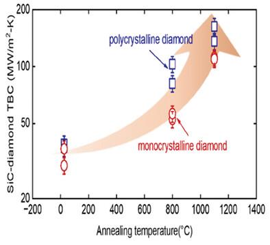
Overheating has emerged as a primary challenge constraining the reliability and performance of next-generation high-performance (ultra)wide bandgap (WBG or UWBG) electronics. Advanced heterogeneous bonding of high-thermal-conductivity WBG thin films and substrates not only constitutes a pivotal technique for fabricating these electronics but also offers potential solutions for thermal management. This study presents the integration of 3C-silicon carbide (SiC) thin films and diamond substrates through a surface-activated bonding technique. Notably, following annealing, the interfaces between 3C-SiC and diamond demonstrate an enhancement in thermal boundary conductance (TBC), reaching up to ≈300%, surpassing all other grown and bonded heterointerfaces. This enhancement is attributed to interfacial reactions, specifically the transformation of amorphous silicon into SiC upon interaction with diamond, which is further corroborated by picosecond ultrasonics measurements. After annealing at 1100 °C, the achieved TBC (150 MW m−2 K−1) is among the highest among all bonded diamond interfaces. Additionally, the visualization of large-area TBC, facilitated by femtosecond laser-based time-domain thermoreflectance measurements, shows the uniformity of the interfaces which are capable of withstanding temperatures as high as 1100 °C. The research marks a significant advancement in the realm of thermally conductive WBG/substrate bonding, which is promising for enhanced cooling of next-generation electronics.

界面反应提高了室温集成半导体界面的导热性,使其温度稳定在 1100 °C 以下
过热已成为制约下一代高性能(超)宽带隙(WBG 或 UWBG)电子器件可靠性和性能的主要挑战。高热导率 WBG 薄膜和基底的先进异质键合技术不仅是制造这些电子器件的关键技术,还为热管理提供了潜在的解决方案。本研究介绍了通过表面活性键合技术将 3C 碳化硅(SiC)薄膜和金刚石基板整合在一起的情况。值得注意的是,退火后,3C-碳化硅和金刚石之间的界面显示出热边界电导(TBC)的增强,最高可达≈300%,超过了所有其他生长和结合的异质界面。这种增强归因于界面反应,特别是无定形硅在与金刚石相互作用时转化为碳化硅,皮秒超声波测量进一步证实了这一点。在 1100 °C 退火后,达到的 TBC(150 MW m-2 K-1)是所有键合金刚石界面中最高的。此外,基于飞秒激光的时域热反射测量可实现大面积 TBC 的可视化,显示出界面的均匀性,能够承受高达 1100 °C 的温度。这项研究标志着导热 WBG/基底键合领域的重大进展,有望增强下一代电子器件的冷却能力。
本文章由计算机程序翻译,如有差异,请以英文原文为准。
求助全文
约1分钟内获得全文
求助全文
来源期刊

Advanced Electronic Materials
NANOSCIENCE & NANOTECHNOLOGYMATERIALS SCIE-MATERIALS SCIENCE, MULTIDISCIPLINARY
CiteScore
11.00
自引率
3.20%
发文量
433
期刊介绍:
Advanced Electronic Materials is an interdisciplinary forum for peer-reviewed, high-quality, high-impact research in the fields of materials science, physics, and engineering of electronic and magnetic materials. It includes research on physics and physical properties of electronic and magnetic materials, spintronics, electronics, device physics and engineering, micro- and nano-electromechanical systems, and organic electronics, in addition to fundamental research.
 求助内容:
求助内容: 应助结果提醒方式:


